M30833FJFP#U3 Renesas Electronics America, M30833FJFP#U3 Datasheet - Page 421
M30833FJFP#U3
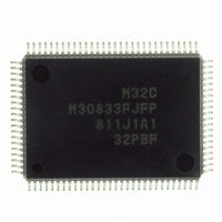
Manufacturer Part Number
M30833FJFP#U3
Description
IC M32C/83 MCU FLASH 100QFP
Manufacturer
Renesas Electronics America
Series
M16C™ M32C/80r
Datasheets
1.M3087BFLGPU3.pdf
(364 pages)
2.M30833FJGPU3.pdf
(96 pages)
3.M30833FJGPU3.pdf
(529 pages)
Specifications of M30833FJFP#U3
Core Processor
M32C/80
Core Size
16/32-Bit
Speed
32MHz
Connectivity
CAN, I²C, IEBus, SIO, UART/USART
Peripherals
DMA, WDT
Number Of I /o
85
Program Memory Size
512KB (512K x 8)
Program Memory Type
FLASH
Ram Size
31K x 8
Voltage - Supply (vcc/vdd)
3 V ~ 5.5 V
Data Converters
A/D 26x10b; D/A 2x8b
Oscillator Type
Internal
Operating Temperature
-40°C ~ 85°C
Package / Case
100-QFP
For Use With
R0K330879S001BE - KIT DEV RSK M32C/87R0K330879S000BE - KIT DEV RSK M32C/87
Lead Free Status / RoHS Status
Lead free / RoHS Compliant
Eeprom Size
-
Available stocks
Company
Part Number
Manufacturer
Quantity
Price


R
R
M
e
E
3
. v
J
2
0
1
9
C
3 .
B
8 /
25.3.1.4 FMR03 Bit
25.3.1.5 FMR05 Bit
0
1
25.3.1.3 FMR02 Bit
3
0
The lock bit set for each block can be disabled by setting the FMR02 bit to "1" (lock bit disabled).
(Refer to 25.3.3 Data Protect Function.) The lock bit is enabled by setting the FMR02 bit to "0" (lock
bit enabled). The FMR02 bit can be set when the FMR01 bit is set to "1". To set the FMR02 bit to "1",
set it to "1" immediately after setting it to "0". To set the FMR02 bit to "0", set it to "0".
The FMR02 bit does not change the lock bit state, but disables the lock bit function. If the block erase
or erase all unlocked block command is executed while the FMR02 bit is set to "1", the lock bit state
changes "0" (locked) to "1" (unlocked) after command execution is completed.
By setting the FMR03 bit to "0" following "1", access to the user ROM area is interrupted to reset the
flash memory control circuit. The flash memory enters read array mode after reset. The FMR00 bit is
set to "1" (READY) and the Status register is set to "80
When the FMR03 bit resets the flash memory control circuit during an auto write or auto erase opera-
tion, an auto write or auto erase operation is interrupted. Data in the block is invalid.
To set the FMR03 bit to "0", set it to "0" immediately after setting it to "1".
The FMR05 bit selects the boot ROM or user ROM area in boot mode. Set to "0" to access (read) the
boot ROM area or to "1" (user ROM access) to access (read, write or erase) the user ROM area.
Execute an instruction written to the FMR05 bit in a space (internal RAM, etc.) other than the flash
memory.
In modes other than boot mode, the user ROM area is accessed (read) regardless of the FMR05 bit
setting.
3
J
G
4
a
0 -
n
o r
3 .
1
u
, 1
3
p
1
2
(
M
0
0
3
6
2
C
8 /
Page 396
, 3
M
3
2
C
f o
8 /
4
3
8
) T
8
16
". (Refer to 25.3.2 Status Register.)
25. Flash Memory Version
Related parts for M30833FJFP#U3
Image
Part Number
Description
Manufacturer
Datasheet
Request
R

Part Number:
Description:
KIT STARTER FOR M16C/29
Manufacturer:
Renesas Electronics America
Datasheet:

Part Number:
Description:
KIT STARTER FOR R8C/2D
Manufacturer:
Renesas Electronics America
Datasheet:

Part Number:
Description:
R0K33062P STARTER KIT
Manufacturer:
Renesas Electronics America
Datasheet:

Part Number:
Description:
KIT STARTER FOR R8C/23 E8A
Manufacturer:
Renesas Electronics America
Datasheet:

Part Number:
Description:
KIT STARTER FOR R8C/25
Manufacturer:
Renesas Electronics America
Datasheet:

Part Number:
Description:
KIT STARTER H8S2456 SHARPE DSPLY
Manufacturer:
Renesas Electronics America
Datasheet:

Part Number:
Description:
KIT STARTER FOR R8C38C
Manufacturer:
Renesas Electronics America
Datasheet:

Part Number:
Description:
KIT STARTER FOR R8C35C
Manufacturer:
Renesas Electronics America
Datasheet:

Part Number:
Description:
KIT STARTER FOR R8CL3AC+LCD APPS
Manufacturer:
Renesas Electronics America
Datasheet:
Part Number:
Description:
KIT STARTER FOR RX610
Manufacturer:
Renesas Electronics America
Datasheet:

Part Number:
Description:
KIT STARTER FOR R32C/118
Manufacturer:
Renesas Electronics America
Datasheet:

Part Number:
Description:
KIT DEV RSK-R8C/26-29
Manufacturer:
Renesas Electronics America
Datasheet:

Part Number:
Description:
KIT STARTER FOR SH7124
Manufacturer:
Renesas Electronics America
Datasheet:

Part Number:
Description:
KIT STARTER FOR H8SX/1622
Manufacturer:
Renesas Electronics America
Datasheet:

Part Number:
Description:
KIT DEV FOR SH7203
Manufacturer:
Renesas Electronics America
Datasheet: