M30833FJFP#U3 Renesas Electronics America, M30833FJFP#U3 Datasheet - Page 217
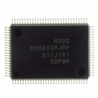
M30833FJFP#U3
Manufacturer Part Number
M30833FJFP#U3
Description
IC M32C/83 MCU FLASH 100QFP
Manufacturer
Renesas Electronics America
Series
M16C™ M32C/80r
Datasheets
1.M3087BFLGPU3.pdf
(364 pages)
2.M30833FJGPU3.pdf
(96 pages)
3.M30833FJGPU3.pdf
(529 pages)
Specifications of M30833FJFP#U3
Core Processor
M32C/80
Core Size
16/32-Bit
Speed
32MHz
Connectivity
CAN, I²C, IEBus, SIO, UART/USART
Peripherals
DMA, WDT
Number Of I /o
85
Program Memory Size
512KB (512K x 8)
Program Memory Type
FLASH
Ram Size
31K x 8
Voltage - Supply (vcc/vdd)
3 V ~ 5.5 V
Data Converters
A/D 26x10b; D/A 2x8b
Oscillator Type
Internal
Operating Temperature
-40°C ~ 85°C
Package / Case
100-QFP
For Use With
R0K330879S001BE - KIT DEV RSK M32C/87R0K330879S000BE - KIT DEV RSK M32C/87
Lead Free Status / RoHS Status
Lead free / RoHS Compliant
Eeprom Size
-
Available stocks
Company
Part Number
Manufacturer
Quantity
Price


R
R
M
e
E
3
. v
J
Figure 16.15 Receive Operation
Table 16.11 Bit Rate
2
0
16.2.1 Bit Rate
1
9
C
B
3 .
B
b (
t i
In UART mode, bit rate is clock frequency which is divided by a setting value of the UiBRG (i=0 to 4)
register and again divided by 16. Table 16.11 lists an example of bit rate setting.
8 /
1
1
2
3
3
5
0
1
R
p
1
2
4
9
4
9
8
1
8
1
3
0
) s
a
2
4
8
6
4
2
8
2
4
2
3
8-bit Data Reception Timing (with no parity and 1 stop bit)
J
e t
0
0
0
0
0
0
0
5
0
0
G
RI bit in UiC1
register
Count Source set
in UiBRG register
RxDi
Transfer Clock
RTSi
IR bit in SiRIC
register
RE bit in UiC1
register
4
a
0
0
0
0
0
0
0
0
0
0
0 -
n
o r
3 .
1
u
S
U
, 1
3
C
p
o
1
B i
o
f o
8 f
8 f
8 f
u
1 f
1 f
1 f
1 f
1 f
1 f
1 f
2
(
u
R
c r
M
0
t n
G
0
e
3
6
2
C
i=0 to 4
NOTES:
S
Page 192
8 /
"1"
"0"
"1"
"0"
"H"
"L"
"1"
"0"
f o
t e
P
1. The above applies when the PRYE bit in the UiMR register is set to "0" (parity disabled),
, 3
U
n i t
r e
Start receiving when the transfer clock is
generated on the falling edge of the start bit
1
1
the SRPS bit in the UiMR register is set to "0" (1 stop bit) and the CRS bit in the UiC0 register is set
to "1" (RTS function selected).
B i
3
0
5
2
0
6
5
3
2
1
g
p i
M
R
1
3
1
5
3
8
1
4
5
9
h
V
: G
1 (
3
6 (
3 (
1 (
6 (
4 (
3 (
2 (
1 (
1 (
r e
a
u l
2
F
7
3
9
7
4
3
2
9
3
l a
n
C
e
1
) h
) h
) h
) h
) h
) h
) h
) h
) h
) h
f o
F
6
8 /
M
u
4
Start bit
n
3
H
8
A
t c
) T
8
z
c
o i
u t
n
l a
b (
Determine if it
is "L"
C
B
p
o l
t i
) s
1
3
3
5
1
2
c
R
1
2
4
9
4
1
8
0
9
8
: k
2
4
8
6
4
2
4
0
a
2
5
e t
0
0
0
1
9
5
6
0
Set to "0" by an interrupt request acknowledgement or by program
3
7
2
4
8
5
3
0
2
0
1
1
S
f o
t e
P
U
n i t
r e
D
1
1
1
B i
2
4
5
7
3
5
0
7
5
3
0
p i
g
8
R
7
5
7
8
5
3
7
1
8
h
V
: G
1 (
Capture a received data
9 (
4 (
2 (
9 (
6 (
4 (
3 (
2 (
2 (
r e
a
Data is transferred from the URTi receive
register to the UiRB register
u l
C
F
6
6
6
6
7
6
3
6
l a
n
e
2
) h
) h
) h
) h
) h
) h
) h
) h
) h
) h
Change to "L" by reading the UiRB register
F
4
M
u
n
H
A
t c
z
c
o i
u t
D
n
l a
1
b (
C
B
p
o l
) s
t i
2
5
1
3
3
1
c
R
2
8
1
1
4
9
4
1
8
9
D
: k
2
4
8
6
8
2
4
7
a
4
2
7
e t
0
0
0
1
4
5
6
2
2
3
2
4
8
5
6
0
2
4
3
1
S
f o
P
t e
Stop bit
r e
U
n i t
2
2
1
1
1
B i
p i
0
0
3
6
0
5
0
6
5
3
g
7
7
R
8
3
h
3
1
3
8
1
8
V
r e
: G
(
(
8 (
6 (
3 (
6 (
4 (
3 (
3 (
2 (
a
C
C
l a
u l
F
F
A
F
7
3
7
4
3
6
3
n
e
) h
) h
) h
) h
) h
) h
) h
) h
) h
) h
F
2
M
u
16. Serial I/O (UART)
n
H
A
t c
z
c
o i
u t
n
l a
b (
C
B
p
o l
t i
) s
1
2
3
3
5
1
2
c
1
4
9
4
8
1
8
1
9
R
4
: k
2
8
6
3
9
2
4
2
2
a
0
0
0
1
8
8
5
6
8
3
e t
4
2
8
5
8
6
0
2
2
1
Related parts for M30833FJFP#U3
Image
Part Number
Description
Manufacturer
Datasheet
Request
R

Part Number:
Description:
KIT STARTER FOR M16C/29
Manufacturer:
Renesas Electronics America
Datasheet:

Part Number:
Description:
KIT STARTER FOR R8C/2D
Manufacturer:
Renesas Electronics America
Datasheet:

Part Number:
Description:
R0K33062P STARTER KIT
Manufacturer:
Renesas Electronics America
Datasheet:

Part Number:
Description:
KIT STARTER FOR R8C/23 E8A
Manufacturer:
Renesas Electronics America
Datasheet:

Part Number:
Description:
KIT STARTER FOR R8C/25
Manufacturer:
Renesas Electronics America
Datasheet:

Part Number:
Description:
KIT STARTER H8S2456 SHARPE DSPLY
Manufacturer:
Renesas Electronics America
Datasheet:

Part Number:
Description:
KIT STARTER FOR R8C38C
Manufacturer:
Renesas Electronics America
Datasheet:

Part Number:
Description:
KIT STARTER FOR R8C35C
Manufacturer:
Renesas Electronics America
Datasheet:

Part Number:
Description:
KIT STARTER FOR R8CL3AC+LCD APPS
Manufacturer:
Renesas Electronics America
Datasheet:
Part Number:
Description:
KIT STARTER FOR RX610
Manufacturer:
Renesas Electronics America
Datasheet:

Part Number:
Description:
KIT STARTER FOR R32C/118
Manufacturer:
Renesas Electronics America
Datasheet:

Part Number:
Description:
KIT DEV RSK-R8C/26-29
Manufacturer:
Renesas Electronics America
Datasheet:

Part Number:
Description:
KIT STARTER FOR SH7124
Manufacturer:
Renesas Electronics America
Datasheet:

Part Number:
Description:
KIT STARTER FOR H8SX/1622
Manufacturer:
Renesas Electronics America
Datasheet:

Part Number:
Description:
KIT DEV FOR SH7203
Manufacturer:
Renesas Electronics America
Datasheet: