M30833FJFP#U3 Renesas Electronics America, M30833FJFP#U3 Datasheet - Page 300
M30833FJFP#U3
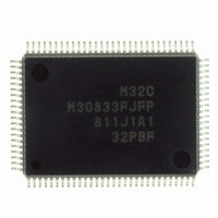
Manufacturer Part Number
M30833FJFP#U3
Description
IC M32C/83 MCU FLASH 100QFP
Manufacturer
Renesas Electronics America
Series
M16C™ M32C/80r
Datasheets
1.M3087BFLGPU3.pdf
(364 pages)
2.M30833FJGPU3.pdf
(96 pages)
3.M30833FJGPU3.pdf
(529 pages)
Specifications of M30833FJFP#U3
Core Processor
M32C/80
Core Size
16/32-Bit
Speed
32MHz
Connectivity
CAN, I²C, IEBus, SIO, UART/USART
Peripherals
DMA, WDT
Number Of I /o
85
Program Memory Size
512KB (512K x 8)
Program Memory Type
FLASH
Ram Size
31K x 8
Voltage - Supply (vcc/vdd)
3 V ~ 5.5 V
Data Converters
A/D 26x10b; D/A 2x8b
Oscillator Type
Internal
Operating Temperature
-40°C ~ 85°C
Package / Case
100-QFP
For Use With
R0K330879S001BE - KIT DEV RSK M32C/87R0K330879S000BE - KIT DEV RSK M32C/87
Lead Free Status / RoHS Status
Lead free / RoHS Compliant
Eeprom Size
-
Available stocks
Company
Part Number
Manufacturer
Quantity
Price


R
R
M
e
E
3
. v
J
2
0
Table 21.7 Pin Settings for Waveform Generation Function (2/2)
NOTES:
Table 21.8 Waveform Generation Function Associated Register Settings
Bit configurations and functions vary with channels and groups used.
Set registers associated with the waveform generation function after setting registers associated with the base timer.
NOTES:
P13
P13
P13
P13
P13
P13
P14
P14
P14
P14
P15
P15
P15
P15
GiPOCRj
G2BCR1
G3BCR1
GiPOj
G3MK4 to
G3MK7
GiFS
GiFE
G2RTP
G3RTP
i = 0 to 3; j = 0 to 7
1
C
9
3 .
B
1. This port is provided in the 144-pin package only.
2. When the CAS bit in the GiBCR1 register is set to "1" (32-bit time measurement function), the OUTC1j pin (j=0 to 7)
1. This bit is in the G2POCRj and G3POCRj registers only.
8 /
Register
0
1
2
3
4
5
6
7
0
1
2
3
0
1
4
5
3
0
Pin
outputs a waveform and the OUTC0k pin (k=0, 1, 4, 5), set as above, outputs a 16-bit low-order waveform.
/OUTC2
/OUTC2
/OUTC2
/OUTC2
/OUTC2
/OUTC2
/OUTC1
/OUTC1
/OUTC1
/OUTC1
/OUTC0
/OUTC0
/OUTC0
/OUTC0
3
J
G
4
a
0 -
n
o r
3 .
1
u
, 1
3
p
1
6 (1)
3 (1)
0 (1)
2 (1)
1 (1)
7 (1)
4 (1,2)
5 (1,2)
6 (1,2)
7 (1,2)
0 (1,2)
1 (1,2)
4 (1,2)
5 (1,2)
2
(
M
0
0
MOD2 to MOD0
PRT
IVL
RLD
RTP
INV
-
RTP0 to
RTP7
3
PRP
-
FSCj
IFEj
6
2
C
PS0 to PS2, PS5 to PS9 Registers PSL0, PSL1, PSL2, PSL3 Registers
PS7_2 = 1
PS7_3 = 1
PS7_4 = 1
PS7_5 = 1
PS7_6 = 1
PS7_7 = 1
PS8_0 = 1
PS8_1 = 1
PS8_2 = 1
PS8_3 = 1
PS9_0 = 1
PS9_1 = 1
PS9_4 = 1
PS9_5= 1
Page 275
(1)
(1)
8 /
, 3
Bit
M
3
2
C
f o
8 /
4
3
8
) T
8
Select waveform output mode
Set to "1" when using the parallel RTP output mode
Select default value
Select reload timing of GiPOj register value
Set to "1" when using the RTP output or the parallel RTP output mode
MOD2 to MOD0 bits are invalid when the RTP bit is set to "1"
Select inversed output
Set to "1" when using the parallel RTP output mode
Select output waveform inverse timing
Set masked values of the base timer and G3PO4 to G3PO7 registers
Set to "0" (waveform generation function) (group 0 and 1 only)
Set to "1" (enables channel j function)
Set RTP output value in RTP output or parallel RTP output mode
(group 3 only)
-
-
-
Bit and Setting
21. Intelligent I/O (Waveform Generation Function)
Function
PSC Register
-
-
-
Related parts for M30833FJFP#U3
Image
Part Number
Description
Manufacturer
Datasheet
Request
R

Part Number:
Description:
KIT STARTER FOR M16C/29
Manufacturer:
Renesas Electronics America
Datasheet:

Part Number:
Description:
KIT STARTER FOR R8C/2D
Manufacturer:
Renesas Electronics America
Datasheet:

Part Number:
Description:
R0K33062P STARTER KIT
Manufacturer:
Renesas Electronics America
Datasheet:

Part Number:
Description:
KIT STARTER FOR R8C/23 E8A
Manufacturer:
Renesas Electronics America
Datasheet:

Part Number:
Description:
KIT STARTER FOR R8C/25
Manufacturer:
Renesas Electronics America
Datasheet:

Part Number:
Description:
KIT STARTER H8S2456 SHARPE DSPLY
Manufacturer:
Renesas Electronics America
Datasheet:

Part Number:
Description:
KIT STARTER FOR R8C38C
Manufacturer:
Renesas Electronics America
Datasheet:

Part Number:
Description:
KIT STARTER FOR R8C35C
Manufacturer:
Renesas Electronics America
Datasheet:

Part Number:
Description:
KIT STARTER FOR R8CL3AC+LCD APPS
Manufacturer:
Renesas Electronics America
Datasheet:
Part Number:
Description:
KIT STARTER FOR RX610
Manufacturer:
Renesas Electronics America
Datasheet:

Part Number:
Description:
KIT STARTER FOR R32C/118
Manufacturer:
Renesas Electronics America
Datasheet:

Part Number:
Description:
KIT DEV RSK-R8C/26-29
Manufacturer:
Renesas Electronics America
Datasheet:

Part Number:
Description:
KIT STARTER FOR SH7124
Manufacturer:
Renesas Electronics America
Datasheet:

Part Number:
Description:
KIT STARTER FOR H8SX/1622
Manufacturer:
Renesas Electronics America
Datasheet:

Part Number:
Description:
KIT DEV FOR SH7203
Manufacturer:
Renesas Electronics America
Datasheet: