M30833FJFP#U3 Renesas Electronics America, M30833FJFP#U3 Datasheet - Page 286
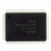
M30833FJFP#U3
Manufacturer Part Number
M30833FJFP#U3
Description
IC M32C/83 MCU FLASH 100QFP
Manufacturer
Renesas Electronics America
Series
M16C™ M32C/80r
Datasheets
1.M3087BFLGPU3.pdf
(364 pages)
2.M30833FJGPU3.pdf
(96 pages)
3.M30833FJGPU3.pdf
(529 pages)
Specifications of M30833FJFP#U3
Core Processor
M32C/80
Core Size
16/32-Bit
Speed
32MHz
Connectivity
CAN, I²C, IEBus, SIO, UART/USART
Peripherals
DMA, WDT
Number Of I /o
85
Program Memory Size
512KB (512K x 8)
Program Memory Type
FLASH
Ram Size
31K x 8
Voltage - Supply (vcc/vdd)
3 V ~ 5.5 V
Data Converters
A/D 26x10b; D/A 2x8b
Oscillator Type
Internal
Operating Temperature
-40°C ~ 85°C
Package / Case
100-QFP
For Use With
R0K330879S001BE - KIT DEV RSK M32C/87R0K330879S000BE - KIT DEV RSK M32C/87
Lead Free Status / RoHS Status
Lead free / RoHS Compliant
Eeprom Size
-
Available stocks
Company
Part Number
Manufacturer
Quantity
Price


R
R
M
e
E
3
. v
J
2
Figure 21.13 G0PO0 to G0PO7, G1PO0 to G1PO7, G2PO0 to G2PO7, G3PO0 to G3PO7 Registers
0
1
C
9
3 .
B
8 /
0
1
3
0
3
J
G
4
a
b15
Group i Waveform Generation Register j (i=0 to 3; j=0 to 7)
0 -
n
o r
b15
Group 3 Waveform Generation Mask Register j (j=4 to 7)
3 .
1
u
NOTES:
, 1
3
p
1
1. This function is enabled in single-phase waveform output mode or phase-delayed waveform output
2
(
M
and G3MK4 to G3MK7 Registers
0
mode. Set the G3MKi register to "0000
0
3
6
b8
2
b8
C
b7
Page 261
8 /
b7
, 3
M
3
2
b0
C
b0
f o
8 /
• When the RLD bit in the GiPOCRj register is set
• When the RLD bit is set to "1",
4
Symbol
G0PO0 to G0PO2
G0PO3 to G0PO5
G0PO6 to G0PO7
G1PO0 to G1PO2
G1PO3 to G1PO5
G1PO6 to G1PO7
G2PO0 to G2PO2
G2PO3 to G2PO5
G2PO6 to G2PO7
G3PO0 to G3PO2
G3PO3 to G3PO5
G3PO6 to G3PO7
value written is immediately reloaded into the
the value is reloaded when the base timer is
to "0",
GiPOj register to output, for example, a waveform
reflecting the value
reset. The value written can be read until reload.
When one or more bit k (k=0 to 15) in this
register is set to "1", the bit k in the group 3 base
timer is masked. The masked value is compared
to the G3POj register
3
8
) T
8
Symbol
G3MK4, G3MK5
G3MK6, G3MK7
Function
16
00C1
00C7
00CD
0101
0107
010D
0141
0147
014D
0181
0187
018D
Function
Address
" in other modes.
(1)
16
16
16
16
16
16
Address
0199
019D
16
16
16
16
16
16
.
-0100
-0106
-0140
-0146
-0180
-0186
-00C0
-00C6
-010C
-014C
-018C
-00CC
16
16
-0198
-019C
16,
16,
16,
16,
16,
16,
16,
16,
16,
16,
16,
16,
0103
0109
0143
0149
0183
0189
00C3
00C9
010F
014F
018F
00CF
16
16
, 019B
, 019F
16
16
16
16
16
16
16
16
16
16
16
-0102
-0108
-0142
-0148
-0182
-0188
16
-010E
-014E
-018E
-00C2
-00C8
-00CE
16
16
-019A
16,
16,
16,
16,
16,
16,
-019E
16
16
16
16,
16,
16
0105
010B
0145
014B
0185
018B
00C5
00CB
16
16
16
16
16
16
16
16
0000
16
-0104
-0144
-0184
16
-010A
-014A
-018A
Setting Range
0000
-00C4
-00CA
Setting Range
After Reset
Indeterminate
Indeterminate
16
16
16
16
16
16
16
16
16
to FFFF
16
to FFFF
After Reset
Indeterminate
Indeterminate
Indeterminate
Indeterminate
Indeterminate
Indeterminate
Indeterminate
Indeterminate
Indeterminate
Indeterminate
Indeterminate
Indeterminate
16
16
21. Intelligent I/O
RW
RW
RW
RW
Related parts for M30833FJFP#U3
Image
Part Number
Description
Manufacturer
Datasheet
Request
R

Part Number:
Description:
KIT STARTER FOR M16C/29
Manufacturer:
Renesas Electronics America
Datasheet:

Part Number:
Description:
KIT STARTER FOR R8C/2D
Manufacturer:
Renesas Electronics America
Datasheet:

Part Number:
Description:
R0K33062P STARTER KIT
Manufacturer:
Renesas Electronics America
Datasheet:

Part Number:
Description:
KIT STARTER FOR R8C/23 E8A
Manufacturer:
Renesas Electronics America
Datasheet:

Part Number:
Description:
KIT STARTER FOR R8C/25
Manufacturer:
Renesas Electronics America
Datasheet:

Part Number:
Description:
KIT STARTER H8S2456 SHARPE DSPLY
Manufacturer:
Renesas Electronics America
Datasheet:

Part Number:
Description:
KIT STARTER FOR R8C38C
Manufacturer:
Renesas Electronics America
Datasheet:

Part Number:
Description:
KIT STARTER FOR R8C35C
Manufacturer:
Renesas Electronics America
Datasheet:

Part Number:
Description:
KIT STARTER FOR R8CL3AC+LCD APPS
Manufacturer:
Renesas Electronics America
Datasheet:
Part Number:
Description:
KIT STARTER FOR RX610
Manufacturer:
Renesas Electronics America
Datasheet:

Part Number:
Description:
KIT STARTER FOR R32C/118
Manufacturer:
Renesas Electronics America
Datasheet:

Part Number:
Description:
KIT DEV RSK-R8C/26-29
Manufacturer:
Renesas Electronics America
Datasheet:

Part Number:
Description:
KIT STARTER FOR SH7124
Manufacturer:
Renesas Electronics America
Datasheet:

Part Number:
Description:
KIT STARTER FOR H8SX/1622
Manufacturer:
Renesas Electronics America
Datasheet:

Part Number:
Description:
KIT DEV FOR SH7203
Manufacturer:
Renesas Electronics America
Datasheet: