M30833FJFP#U3 Renesas Electronics America, M30833FJFP#U3 Datasheet - Page 348
M30833FJFP#U3
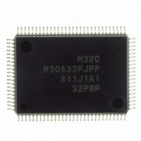
Manufacturer Part Number
M30833FJFP#U3
Description
IC M32C/83 MCU FLASH 100QFP
Manufacturer
Renesas Electronics America
Series
M16C™ M32C/80r
Datasheets
1.M3087BFLGPU3.pdf
(364 pages)
2.M30833FJGPU3.pdf
(96 pages)
3.M30833FJGPU3.pdf
(529 pages)
Specifications of M30833FJFP#U3
Core Processor
M32C/80
Core Size
16/32-Bit
Speed
32MHz
Connectivity
CAN, I²C, IEBus, SIO, UART/USART
Peripherals
DMA, WDT
Number Of I /o
85
Program Memory Size
512KB (512K x 8)
Program Memory Type
FLASH
Ram Size
31K x 8
Voltage - Supply (vcc/vdd)
3 V ~ 5.5 V
Data Converters
A/D 26x10b; D/A 2x8b
Oscillator Type
Internal
Operating Temperature
-40°C ~ 85°C
Package / Case
100-QFP
For Use With
R0K330879S001BE - KIT DEV RSK M32C/87R0K330879S000BE - KIT DEV RSK M32C/87
Lead Free Status / RoHS Status
Lead free / RoHS Compliant
Eeprom Size
-
Available stocks
Company
Part Number
Manufacturer
Quantity
Price


M
R
R
e
E
3
. v
J
2
Figure 21. 51 Transmit and Receive Operation (16-bit Length)
0
C
1
9
3 .
8 /
B
0
1
3
Base Timer 3
ISCLK3 pin output
(transmit clock in the
channel 2 WG function)
ISTxD3 pin output
(data to be transmitted)
SIO3TR bit
when IRS=0
(no data in the
transmit buffer)
SIO3TR bit
when IRS=1
(transmission completed)
ISRxD3 pin input
(received data)
SIO3RR bit
0
3
G
J
The above timing applies under the following settings.
4
a
o r
0 -
n
• The CKDIR bit in the G3MR register is set to "0" (internal clock)
• The UFORM bit in the G3MR register is set to "0" (LSB first)
• The IPOL bit and OPOL bit in the G3CR register are set to "0" (no inverse)
• The TLD bit in the G3CR register is set to "1" (16 bits long)
3 .
u
1
p
, 1
3
1
(
2
M
0
3
0
2
6
C
Write to the G3TB register
m
n+2
8 /
Page 323
, 3
M
3
2
C
f o
8 /
Write "0" by program
if setting to "0"
4
3
Bit 0
Bit 0
The base timer is reset by the channel 0
waveform generation function
8
) T
8
Bit 1
Bit 1
21. Intelligent I/O (Group 3 Communication Function)
Bit 2
Bit 2
Bit 14
Bit 14
Write "0" by program if setting to "0"
n : Setting value of the G3PO0 register
m : Setting value of the G3PO2 register
SIO3TR bit : Bit in the IIO10IR register
SIO3RR bit : Bit in the IIO9IR register
IRS bit
: Bit in the G3MR register
Bit 15
Bit 15
Write "0" by program
if setting to "0"
Related parts for M30833FJFP#U3
Image
Part Number
Description
Manufacturer
Datasheet
Request
R

Part Number:
Description:
KIT STARTER FOR M16C/29
Manufacturer:
Renesas Electronics America
Datasheet:

Part Number:
Description:
KIT STARTER FOR R8C/2D
Manufacturer:
Renesas Electronics America
Datasheet:

Part Number:
Description:
R0K33062P STARTER KIT
Manufacturer:
Renesas Electronics America
Datasheet:

Part Number:
Description:
KIT STARTER FOR R8C/23 E8A
Manufacturer:
Renesas Electronics America
Datasheet:

Part Number:
Description:
KIT STARTER FOR R8C/25
Manufacturer:
Renesas Electronics America
Datasheet:

Part Number:
Description:
KIT STARTER H8S2456 SHARPE DSPLY
Manufacturer:
Renesas Electronics America
Datasheet:

Part Number:
Description:
KIT STARTER FOR R8C38C
Manufacturer:
Renesas Electronics America
Datasheet:

Part Number:
Description:
KIT STARTER FOR R8C35C
Manufacturer:
Renesas Electronics America
Datasheet:

Part Number:
Description:
KIT STARTER FOR R8CL3AC+LCD APPS
Manufacturer:
Renesas Electronics America
Datasheet:
Part Number:
Description:
KIT STARTER FOR RX610
Manufacturer:
Renesas Electronics America
Datasheet:

Part Number:
Description:
KIT STARTER FOR R32C/118
Manufacturer:
Renesas Electronics America
Datasheet:

Part Number:
Description:
KIT DEV RSK-R8C/26-29
Manufacturer:
Renesas Electronics America
Datasheet:

Part Number:
Description:
KIT STARTER FOR SH7124
Manufacturer:
Renesas Electronics America
Datasheet:

Part Number:
Description:
KIT STARTER FOR H8SX/1622
Manufacturer:
Renesas Electronics America
Datasheet:

Part Number:
Description:
KIT DEV FOR SH7203
Manufacturer:
Renesas Electronics America
Datasheet: