M30833FJFP#U3 Renesas Electronics America, M30833FJFP#U3 Datasheet - Page 425
M30833FJFP#U3
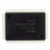
Manufacturer Part Number
M30833FJFP#U3
Description
IC M32C/83 MCU FLASH 100QFP
Manufacturer
Renesas Electronics America
Series
M16C™ M32C/80r
Datasheets
1.M3087BFLGPU3.pdf
(364 pages)
2.M30833FJGPU3.pdf
(96 pages)
3.M30833FJGPU3.pdf
(529 pages)
Specifications of M30833FJFP#U3
Core Processor
M32C/80
Core Size
16/32-Bit
Speed
32MHz
Connectivity
CAN, I²C, IEBus, SIO, UART/USART
Peripherals
DMA, WDT
Number Of I /o
85
Program Memory Size
512KB (512K x 8)
Program Memory Type
FLASH
Ram Size
31K x 8
Voltage - Supply (vcc/vdd)
3 V ~ 5.5 V
Data Converters
A/D 26x10b; D/A 2x8b
Oscillator Type
Internal
Operating Temperature
-40°C ~ 85°C
Package / Case
100-QFP
For Use With
R0K330879S001BE - KIT DEV RSK M32C/87R0K330879S000BE - KIT DEV RSK M32C/87
Lead Free Status / RoHS Status
Lead free / RoHS Compliant
Eeprom Size
-
Available stocks
Company
Part Number
Manufacturer
Quantity
Price


R
R
M
e
E
3
. v
J
2
0
25.3.5 Software Commands
Read or write commands and data from or to even addresses in the user ROM area, in 16-bit units. When
writing a command code, 8 high-order bits (D
1
9
C
3 .
B
8 /
0
1
25.3.5.1 Read Array Command
25.3.5.2 Read Status Register Command
25.3.5.3 Clear Status Register Command
25.3.5.4 Page Program Command
3
0
The read array command reads the flash memory.
Read array mode is entered by writing command code "xxFF
specified address can be read after the next bus cycle.
The microcomputer remains in read array mode until another command is written. Therefore, contents
from multiple addresses can be read consecutively.
The read status register command reads the status register (refer to 25.3.7 Status Register for details).
By writing command code "xx70
bus cycle. Read an even address in the user ROM area.
The clear status register command clears the status register. By writing "xx50
the SR5 to SR3 bits in the status register (see Table 25.4) are set to "0".
The page program command executes programs in 128-word (256-byte) units.
After writing command code "xx41
cycles in 16-bit units. Increment by two, from "00
Auto write, programming and verification of data, is performed when 128 word data has been written.
Do not access the flash memory or execute the next command during auto write operation.
The FMR00 bit in the FMR0 register indicates whether an auto program operation is completed.
After an auto write operation is completed, the Status register indicates whether the auto write opera-
tion is completed as expected or not. (Refer to 25.3.6 Full Status Check.)
Figure 25.6 shows a flow chart of the page program command programming. When programming a
space which is already programmed, execute erase (block erase) before programming. If the page
program command is executed to a space already programmed, no program error occurs but the page
is indeterminate.
The lock bit can protect blocks from being programmed. (Refer to 25.3.3 Data Protect Function.)
3
J
G
4
a
0 -
n
o r
3 .
1
u
, 1
3
p
1
2
(
M
0
0
3
6
2
C
8 /
Page 400
, 3
M
3
2
C
f o
8 /
4
3
8
) T
8
16
" in the first bus cycle, the status register can be read in the second
16
" in the first bus cycle, write data to the 2nd through 129th bus
15
to D
8
16
) are ignored.
" to "FE
16
", the 8 low-order bits of the write address.
16
" in the first bus cycle. Content of a
25. Flash Memory Version
16
" in the first bus cycle,
Related parts for M30833FJFP#U3
Image
Part Number
Description
Manufacturer
Datasheet
Request
R

Part Number:
Description:
KIT STARTER FOR M16C/29
Manufacturer:
Renesas Electronics America
Datasheet:

Part Number:
Description:
KIT STARTER FOR R8C/2D
Manufacturer:
Renesas Electronics America
Datasheet:

Part Number:
Description:
R0K33062P STARTER KIT
Manufacturer:
Renesas Electronics America
Datasheet:

Part Number:
Description:
KIT STARTER FOR R8C/23 E8A
Manufacturer:
Renesas Electronics America
Datasheet:

Part Number:
Description:
KIT STARTER FOR R8C/25
Manufacturer:
Renesas Electronics America
Datasheet:

Part Number:
Description:
KIT STARTER H8S2456 SHARPE DSPLY
Manufacturer:
Renesas Electronics America
Datasheet:

Part Number:
Description:
KIT STARTER FOR R8C38C
Manufacturer:
Renesas Electronics America
Datasheet:

Part Number:
Description:
KIT STARTER FOR R8C35C
Manufacturer:
Renesas Electronics America
Datasheet:

Part Number:
Description:
KIT STARTER FOR R8CL3AC+LCD APPS
Manufacturer:
Renesas Electronics America
Datasheet:
Part Number:
Description:
KIT STARTER FOR RX610
Manufacturer:
Renesas Electronics America
Datasheet:

Part Number:
Description:
KIT STARTER FOR R32C/118
Manufacturer:
Renesas Electronics America
Datasheet:

Part Number:
Description:
KIT DEV RSK-R8C/26-29
Manufacturer:
Renesas Electronics America
Datasheet:

Part Number:
Description:
KIT STARTER FOR SH7124
Manufacturer:
Renesas Electronics America
Datasheet:

Part Number:
Description:
KIT STARTER FOR H8SX/1622
Manufacturer:
Renesas Electronics America
Datasheet:

Part Number:
Description:
KIT DEV FOR SH7203
Manufacturer:
Renesas Electronics America
Datasheet: