D6417709SF167BV Renesas Electronics America, D6417709SF167BV Datasheet - Page 287
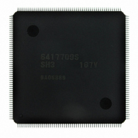
D6417709SF167BV
Manufacturer Part Number
D6417709SF167BV
Description
IC SUPER H MPU ROMLESS 208LQFP
Manufacturer
Renesas Electronics America
Series
SuperH® SH7700r
Datasheet
1.D6417709SBP167BV.pdf
(809 pages)
Specifications of D6417709SF167BV
Core Processor
SH-3
Core Size
32-Bit
Speed
167MHz
Connectivity
EBI/EMI, FIFO, IrDA, SCI, SmartCard
Peripherals
DMA, POR, WDT
Number Of I /o
96
Program Memory Type
ROMless
Ram Size
16K x 8
Voltage - Supply (vcc/vdd)
1.75 V ~ 2.05 V
Data Converters
A/D 8x10b; D/A 2x8b
Oscillator Type
Internal
Operating Temperature
-20°C ~ 75°C
Package / Case
208-LQFP
Lead Free Status / RoHS Status
Lead free / RoHS Compliant
Eeprom Size
-
Program Memory Size
-
Available stocks
Company
Part Number
Manufacturer
Quantity
Price
Company:

Part Number:
D6417709SF167BV
Manufacturer:
Renesas Electronics America
Quantity:
10 000


Bit 15—WAIT Sampling Timing Select (WAITSEL): Specifies the WAIT signal sampling
timing.
Note: * Operation is not guaranteed if WAIT is asserted while WEITSEL = 0.
Bits 14, 3, and 2 —Reserved: These bits are always read as 0. The write value should always be
0.
Bits 2n + 1, 2n—Area n (6–2, 0) Intercycle Idle Specification (AnIW1, AnIW0): Specify the
number of idles inserted between bus cycles when switching between physical space area n (6–2,
0) and another space or between a read access and a write access in the same physical space.
10.2.4
Wait state control register 2 (WCR2) is a 16-bit readable/writable register that specifies the
number of wait state cycles inserted for each area. It also specifies the data access pitch for burst
memory accesses. This allows direct connection of even low-speed memories without an external
circuit. WCR2 is initialized to H'FFFF by a power-on reset. It is not initialized by a manual reset
or in standby mode.
Bit 15: WAITSEL
0
1
Bit 2n + 1: AnIW1
0
1
Initial value:
Initial value:
Wait State Control Register 2 (WCR2)
R/W:
R/W:
Bit:
Bit:
Bit 2n: AnIW0
0
1
0
1
Description
Setting to 1 when using the WAIT signal *
Sampled WAIT signal at fall of CKIO
A6 W2
A4 W0
R/W
R/W
15
1
7
1
A6 W1
A3 W1
R/W
R/W
14
1
6
1
A6 W0
A3 W0
R/W
R/W
Description
1 idle cycle inserted
1 idle cycle inserted
2 idle cycles inserted
3 idle cycles inserted
13
1
5
1
A5 W2
A2 W1
R/W
R/W
12
1
4
1
A5 W1
A2 W0
R/W
R/W
11
1
3
1
Rev. 5.00, 09/03, page 241 of 760
A5 W0
A0 W2
R/W
R/W
10
1
2
1
A4 W2
A0 W1
R/W
R/W
9
1
1
1
(Initial value)
(Initial value)
A4 W1
A0 W0
R/W
R/W
8
1
0
1
Related parts for D6417709SF167BV
Image
Part Number
Description
Manufacturer
Datasheet
Request
R

Part Number:
Description:
KIT STARTER FOR M16C/29
Manufacturer:
Renesas Electronics America
Datasheet:

Part Number:
Description:
KIT STARTER FOR R8C/2D
Manufacturer:
Renesas Electronics America
Datasheet:

Part Number:
Description:
R0K33062P STARTER KIT
Manufacturer:
Renesas Electronics America
Datasheet:

Part Number:
Description:
KIT STARTER FOR R8C/23 E8A
Manufacturer:
Renesas Electronics America
Datasheet:

Part Number:
Description:
KIT STARTER FOR R8C/25
Manufacturer:
Renesas Electronics America
Datasheet:

Part Number:
Description:
KIT STARTER H8S2456 SHARPE DSPLY
Manufacturer:
Renesas Electronics America
Datasheet:

Part Number:
Description:
KIT STARTER FOR R8C38C
Manufacturer:
Renesas Electronics America
Datasheet:

Part Number:
Description:
KIT STARTER FOR R8C35C
Manufacturer:
Renesas Electronics America
Datasheet:

Part Number:
Description:
KIT STARTER FOR R8CL3AC+LCD APPS
Manufacturer:
Renesas Electronics America
Datasheet:
Part Number:
Description:
KIT STARTER FOR RX610
Manufacturer:
Renesas Electronics America
Datasheet:

Part Number:
Description:
KIT STARTER FOR R32C/118
Manufacturer:
Renesas Electronics America
Datasheet:

Part Number:
Description:
KIT DEV RSK-R8C/26-29
Manufacturer:
Renesas Electronics America
Datasheet:

Part Number:
Description:
KIT STARTER FOR SH7124
Manufacturer:
Renesas Electronics America
Datasheet:

Part Number:
Description:
KIT STARTER FOR H8SX/1622
Manufacturer:
Renesas Electronics America
Datasheet:

Part Number:
Description:
KIT DEV FOR SH7203
Manufacturer:
Renesas Electronics America
Datasheet: