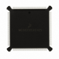
MC68332GVEH25 Freescale Semiconductor, MC68332GVEH25 Datasheet - Page 34

MC68332GVEH25
Manufacturer Part Number
MC68332GVEH25
Description
IC MCU 32BIT 25MHZ 132-PQFP
Manufacturer
Freescale Semiconductor
Series
M683xxr
Specifications of MC68332GVEH25
Core Processor
CPU32
Core Size
32-Bit
Speed
25MHz
Connectivity
EBI/EMI, SCI, SPI, UART/USART
Peripherals
POR, PWM, WDT
Number Of I /o
15
Program Memory Type
ROMless
Ram Size
2K x 8
Voltage - Supply (vcc/vdd)
4.5 V ~ 5.5 V
Oscillator Type
Internal
Operating Temperature
-40°C ~ 105°C
Package / Case
132-QFP
Processor Series
M683xx
Core
CPU32
Data Bus Width
32 bit
Controller Family/series
68K
No. Of I/o's
15
Ram Memory Size
2KB
Cpu Speed
25MHz
No. Of Timers
1
Embedded Interface Type
QSPI, SCI, UART
Digital Ic Case Style
PQFP
Rohs Compliant
Yes
Data Ram Size
2 KB
Interface Type
QSPI, SCI, UART
Maximum Clock Frequency
25 MHz
Number Of Programmable I/os
15
Number Of Timers
16
Maximum Operating Temperature
+ 105 C
Mounting Style
SMD/SMT
Minimum Operating Temperature
- 40 C
Lead Free Status / RoHS Status
Request inventory verification / Request inventory verification
Eeprom Size
-
Program Memory Size
-
Data Converters
-
Lead Free Status / Rohs Status
Lead free / RoHS Compliant
Available stocks
Company
Part Number
Manufacturer
Quantity
Price
Company:
Part Number:
MC68332GVEH25
Manufacturer:
Freescale Semiconductor
Quantity:
135
Company:
Part Number:
MC68332GVEH25
Manufacturer:
Freescale Semiconductor
Quantity:
10 000
- Current page: 34 of 265
- Download datasheet (7Mb)
3.6.1 Internal Register Map
3.6.2 Address Space Maps
3-10
In Figure 3-4, IMB ADDR[23:20] are represented by the letter Y. The value represent-
ed by Y determines the base address of MCU module control registers. In M68300 mi-
crocontrollers, Y is equal to M111, where M is the logic state of the module mapping
(MM) bit in the system integration module configuration register (SIMCR).
Figure 3-5 shows a single memory space. Function codes FC[2:0] are not decoded
externally so that separate user/supervisor or program/data spaces are not provided.
In Figure 3-6, FC2 is decoded, resulting in separate supervisor and user spaces.
FC[1:0] are not decoded, so that separate program and data spaces are not provided.
In Figure 3-7 and Figure 3-8, FC[2:0] are decoded, resulting in four separate memory
spaces: supervisor/program, supervisor/data, user/program and user/data.
All exception vectors are located in supervisor data space, except the reset vector,
which is located in supervisor program space. Only the initial reset vector is fixed in
the processor's memory map. Once initialization is complete, there are no fixed as-
signments. Since the vector base register (VBR) provides the base address of the vec-
tor table, the vector table can be located anywhere in memory. Refer to SECTION 5
CENTRAL PROCESSING UNIT for more information concerning memory manage-
ment, extended addressing, and exception processing. Refer to SECTION 4 SYSTEM
INTEGRATION MODULE for more information concerning function codes and ad-
dress space types.
$YFFA00
$YFFA80
$YFFB00
$YFFB40
$YFFC00
$YFFE00
$YFFFFF
$YFF000
Figure 3-4 Internal Register Memory Map
Freescale Semiconductor, Inc.
TPURAM CONTROL
For More Information On This Product,
RESERVED
RESERVED
TPU
QSM
SIM
Go to: www.freescale.com
OVERVIEW
TPURAM ARRAY
2-KBYTE
332 ADDRESS MAP
USER’S MANUAL
MC68332
Related parts for MC68332GVEH25
Image
Part Number
Description
Manufacturer
Datasheet
Request
R
Part Number:
Description:
Manufacturer:
Freescale Semiconductor, Inc
Datasheet:
Part Number:
Description:
Manufacturer:
Freescale Semiconductor, Inc
Datasheet:
Part Number:
Description:
Manufacturer:
Freescale Semiconductor, Inc
Datasheet:
Part Number:
Description:
Manufacturer:
Freescale Semiconductor, Inc
Datasheet:
Part Number:
Description:
Manufacturer:
Freescale Semiconductor, Inc
Datasheet:
Part Number:
Description:
Manufacturer:
Freescale Semiconductor, Inc
Datasheet:
Part Number:
Description:
Manufacturer:
Freescale Semiconductor, Inc
Datasheet:
Part Number:
Description:
Manufacturer:
Freescale Semiconductor, Inc
Datasheet:
Part Number:
Description:
Manufacturer:
Freescale Semiconductor, Inc
Datasheet:
Part Number:
Description:
Manufacturer:
Freescale Semiconductor, Inc
Datasheet:
Part Number:
Description:
Manufacturer:
Freescale Semiconductor, Inc
Datasheet:
Part Number:
Description:
Manufacturer:
Freescale Semiconductor, Inc
Datasheet:
Part Number:
Description:
Manufacturer:
Freescale Semiconductor, Inc
Datasheet:
Part Number:
Description:
Manufacturer:
Freescale Semiconductor, Inc
Datasheet:
Part Number:
Description:
Manufacturer:
Freescale Semiconductor, Inc
Datasheet:


