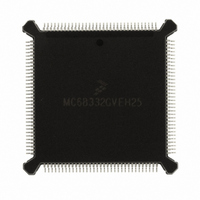
MC68332GVEH25 Freescale Semiconductor, MC68332GVEH25 Datasheet - Page 172

MC68332GVEH25
Manufacturer Part Number
MC68332GVEH25
Description
IC MCU 32BIT 25MHZ 132-PQFP
Manufacturer
Freescale Semiconductor
Series
M683xxr
Specifications of MC68332GVEH25
Core Processor
CPU32
Core Size
32-Bit
Speed
25MHz
Connectivity
EBI/EMI, SCI, SPI, UART/USART
Peripherals
POR, PWM, WDT
Number Of I /o
15
Program Memory Type
ROMless
Ram Size
2K x 8
Voltage - Supply (vcc/vdd)
4.5 V ~ 5.5 V
Oscillator Type
Internal
Operating Temperature
-40°C ~ 105°C
Package / Case
132-QFP
Processor Series
M683xx
Core
CPU32
Data Bus Width
32 bit
Controller Family/series
68K
No. Of I/o's
15
Ram Memory Size
2KB
Cpu Speed
25MHz
No. Of Timers
1
Embedded Interface Type
QSPI, SCI, UART
Digital Ic Case Style
PQFP
Rohs Compliant
Yes
Data Ram Size
2 KB
Interface Type
QSPI, SCI, UART
Maximum Clock Frequency
25 MHz
Number Of Programmable I/os
15
Number Of Timers
16
Maximum Operating Temperature
+ 105 C
Mounting Style
SMD/SMT
Minimum Operating Temperature
- 40 C
Lead Free Status / RoHS Status
Request inventory verification / Request inventory verification
Eeprom Size
-
Program Memory Size
-
Data Converters
-
Lead Free Status / Rohs Status
Lead free / RoHS Compliant
Available stocks
Company
Part Number
Manufacturer
Quantity
Price
Company:
Part Number:
MC68332GVEH25
Manufacturer:
Freescale Semiconductor
Quantity:
135
Company:
Part Number:
MC68332GVEH25
Manufacturer:
Freescale Semiconductor
Quantity:
10 000
- Current page: 172 of 265
- Download datasheet (7Mb)
8.4 TPURAM Privilege Level
8.5 Normal Operation
8.6 Standby Operation
8-2
an address that overlaps the address of the module control register block. Writing a
valid base address to TRAMBAR[15:3] clears RAMDS and enables the array.
TRAMBAR can be written only once after a master reset. This prevents runaway soft-
ware from accidentally re-mapping the array. Because the locking mechanism is acti-
vated by the first write after a master reset, the base address field should be written in
a single word operation. Writing only one-half of the register prevents the other half
from being written. Note that in test mode the locking mechanism for TRAMBAR can
be disabled by the RTBA bit in the TRAMTST register.
The RASP field in TRAMMCR specifies whether access to the TPURAM module can
be made from the supervisor privilege level only or from either the user or supervisor
privilege level. If supervisor-only access is specified, an access from the user privilege
level is ignored by the TPURAM control logic and can be decoded externally. Refer to
SECTION 4 SYSTEM INTEGRATION MODULE and SECTION 5 CENTRAL PRO-
CESSING UNIT for more information concerning privilege levels.
In normal operation, TPURAM is accessed via the IMB by a bus master and is pow-
ered by V
word access takes one bus cycle (two system clock cycles). A long word access re-
quires two bus cycles. Refer to SECTION 4 SYSTEM INTEGRATION MODULE for
more information concerning access times.
During normal operation, the TPU does not access the array and has no effect on the
operation of the TPURAM module.
Standby mode maintains the RAM array when the MCU main power supply is turned
off. Low-power mode allows the central processing unit to control MCU power con-
sumption.
Relative voltage levels of the V
is in standby mode. TPURAM circuitry switches to the standby power source when
specified limits are exceeded. If specified standby supply voltage levels are main-
tained during the transition, there is no loss of memory when switching occurs. The
RAM array cannot be accessed while the TPURAM module is powered from V
If standby operation is not desired, connect the V
I
sition from normal operating level to the level specified for standby operation. This oc-
curs within the voltage range V
when V
Refer to APPENDIX A ELECTRICAL CHARACTERISTICS for standby switching and
power consumption specifications.
To prevent standby supply voltage from going below the specified minimum, a filter ca-
pacitor must be attached between the V
SB
exceeds specified maximum standby current during the time V
DD
DD
» V
. The array can be accessed by byte, word, or long word. A byte or aligned
SB
– 1.5 V, and averages 1.0 mA over the transition period.
Freescale Semiconductor, Inc.
For More Information On This Product,
STANDBY RAM WITH TPU EMULATION
Go to: www.freescale.com
SB
DD
– 0.5 V
and V
STBY
STBY
V
DD
and V
pins determine whether the TPURAM
STBY
V
SS
SS
pins. To calculate filter capac-
pin to the V
+ 0.5 V. Typically, I
DD
SS
makes the tran-
USER’S MANUAL
pin.
SB
MC68332
peaks
STBY
.
Related parts for MC68332GVEH25
Image
Part Number
Description
Manufacturer
Datasheet
Request
R
Part Number:
Description:
Manufacturer:
Freescale Semiconductor, Inc
Datasheet:
Part Number:
Description:
Manufacturer:
Freescale Semiconductor, Inc
Datasheet:
Part Number:
Description:
Manufacturer:
Freescale Semiconductor, Inc
Datasheet:
Part Number:
Description:
Manufacturer:
Freescale Semiconductor, Inc
Datasheet:
Part Number:
Description:
Manufacturer:
Freescale Semiconductor, Inc
Datasheet:
Part Number:
Description:
Manufacturer:
Freescale Semiconductor, Inc
Datasheet:
Part Number:
Description:
Manufacturer:
Freescale Semiconductor, Inc
Datasheet:
Part Number:
Description:
Manufacturer:
Freescale Semiconductor, Inc
Datasheet:
Part Number:
Description:
Manufacturer:
Freescale Semiconductor, Inc
Datasheet:
Part Number:
Description:
Manufacturer:
Freescale Semiconductor, Inc
Datasheet:
Part Number:
Description:
Manufacturer:
Freescale Semiconductor, Inc
Datasheet:
Part Number:
Description:
Manufacturer:
Freescale Semiconductor, Inc
Datasheet:
Part Number:
Description:
Manufacturer:
Freescale Semiconductor, Inc
Datasheet:
Part Number:
Description:
Manufacturer:
Freescale Semiconductor, Inc
Datasheet:
Part Number:
Description:
Manufacturer:
Freescale Semiconductor, Inc
Datasheet:


