MC68332GVEH25 Freescale Semiconductor, MC68332GVEH25 Datasheet - Page 23
MC68332GVEH25
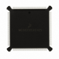
Manufacturer Part Number
MC68332GVEH25
Description
IC MCU 32BIT 25MHZ 132-PQFP
Manufacturer
Freescale Semiconductor
Series
M683xxr
Specifications of MC68332GVEH25
Core Processor
CPU32
Core Size
32-Bit
Speed
25MHz
Connectivity
EBI/EMI, SCI, SPI, UART/USART
Peripherals
POR, PWM, WDT
Number Of I /o
15
Program Memory Type
ROMless
Ram Size
2K x 8
Voltage - Supply (vcc/vdd)
4.5 V ~ 5.5 V
Oscillator Type
Internal
Operating Temperature
-40°C ~ 105°C
Package / Case
132-QFP
Processor Series
M683xx
Core
CPU32
Data Bus Width
32 bit
Controller Family/series
68K
No. Of I/o's
15
Ram Memory Size
2KB
Cpu Speed
25MHz
No. Of Timers
1
Embedded Interface Type
QSPI, SCI, UART
Digital Ic Case Style
PQFP
Rohs Compliant
Yes
Data Ram Size
2 KB
Interface Type
QSPI, SCI, UART
Maximum Clock Frequency
25 MHz
Number Of Programmable I/os
15
Number Of Timers
16
Maximum Operating Temperature
+ 105 C
Mounting Style
SMD/SMT
Minimum Operating Temperature
- 40 C
Lead Free Status / RoHS Status
Request inventory verification / Request inventory verification
Eeprom Size
-
Program Memory Size
-
Data Converters
-
Lead Free Status / Rohs Status
Lead free / RoHS Compliant
Available stocks
Company
Part Number
Manufacturer
Quantity
Price
Company:

Part Number:
MC68332GVEH25
Manufacturer:
Freescale Semiconductor
Quantity:
135
Company:
Part Number:
MC68332GVEH25
Manufacturer:
Freescale Semiconductor
Quantity:
10 000


2.5 Conventions
MC68332
USER’S MANUAL
Logic level one is the voltage that corresponds to a Boolean true (1) state.
Logic level zero is the voltage that corresponds to a Boolean false (0) state.
Set refers specifically to establishing logic level one on a bit or bits.
Clear refers specifically to establishing logic level zero on a bit or bits.
Asserted means that a signal is in active logic state. An active low signal changes
from logic level one to logic level zero when asserted, and an active high signal chang-
es from logic level zero to logic level one.
Negated means that an asserted signal changes logic state. An active low signal
changes from logic level zero to logic level one when negated, and an active high sig-
nal changes from logic level one to logic level zero.
A specific mnemonic within a range is referred to by mnemonic and number. A15 is
bit 15 of accumulator A; ADDR7 is line 7 of the address bus; CSOR0 is chip-select op-
tion register 0. A range of mnemonics is referred to by mnemonic and the numbers
that define the range. AM[35:30] are bits 35 to 30 of accumulator M; CSOR[0:5] are
the first six option registers
Parentheses are used to indicate the content of a register or memory location, rather
than the register or memory location itself. (A) is the content of accumulator A. (M M
LSB means least significant bit or bits. MSB means most significant bit or bits. Refer-
ences to low and high bytes are spelled out.
LSW means least significant word or words. MSW means most significant word or
words.
ADDR is the address bus. ADDR[7:0] are the eight LSB of the address bus.
DATA is the data bus. DATA[15:8] are the eight MSB of the data bus.
1) is the content of the word at address M.
TRAMMCR — TPURAM Module Configuration Register
TRAMBAR — TPURAM Base Address/Status Register
TSTMSRA — Test Module Master Shift Register A
TSTMSRB — Test Module Master Shift Register B
TRAMTST — TPURAM Test Register
TPUMCR — TPU Module Configuration Register
SYNCR — Clock Synthesizer Control Register
SYPCR — System Protection Control Register
TR[0:F] — QSM Transmit Data RAM
TSTRC — Test Module Repetition Counter
TSTSC — Test Module Shift Count Register
SWSR — Software Watchdog Service Register
TICR — TPU Interrupt Configuration Register
TCR — TPU Test Configuration Register
Freescale Semiconductor, Inc.
For More Information On This Product,
Go to: www.freescale.com
NOMENCLATURE
2-5
Related parts for MC68332GVEH25
Image
Part Number
Description
Manufacturer
Datasheet
Request
R

Part Number:
Description:
Manufacturer:
Freescale Semiconductor, Inc
Datasheet:
Part Number:
Description:
Manufacturer:
Freescale Semiconductor, Inc
Datasheet:
Part Number:
Description:
Manufacturer:
Freescale Semiconductor, Inc
Datasheet:
Part Number:
Description:
Manufacturer:
Freescale Semiconductor, Inc
Datasheet:
Part Number:
Description:
Manufacturer:
Freescale Semiconductor, Inc
Datasheet:
Part Number:
Description:
Manufacturer:
Freescale Semiconductor, Inc
Datasheet:
Part Number:
Description:
Manufacturer:
Freescale Semiconductor, Inc
Datasheet:
Part Number:
Description:
Manufacturer:
Freescale Semiconductor, Inc
Datasheet:
Part Number:
Description:
Manufacturer:
Freescale Semiconductor, Inc
Datasheet:
Part Number:
Description:
Manufacturer:
Freescale Semiconductor, Inc
Datasheet:
Part Number:
Description:
Manufacturer:
Freescale Semiconductor, Inc
Datasheet:
Part Number:
Description:
Manufacturer:
Freescale Semiconductor, Inc
Datasheet:
Part Number:
Description:
Manufacturer:
Freescale Semiconductor, Inc
Datasheet:
Part Number:
Description:
Manufacturer:
Freescale Semiconductor, Inc
Datasheet:
Part Number:
Description:
Manufacturer:
Freescale Semiconductor, Inc
Datasheet: