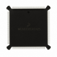
MC68332GVEH25 Freescale Semiconductor, MC68332GVEH25 Datasheet - Page 141

MC68332GVEH25
Manufacturer Part Number
MC68332GVEH25
Description
IC MCU 32BIT 25MHZ 132-PQFP
Manufacturer
Freescale Semiconductor
Series
M683xxr
Specifications of MC68332GVEH25
Core Processor
CPU32
Core Size
32-Bit
Speed
25MHz
Connectivity
EBI/EMI, SCI, SPI, UART/USART
Peripherals
POR, PWM, WDT
Number Of I /o
15
Program Memory Type
ROMless
Ram Size
2K x 8
Voltage - Supply (vcc/vdd)
4.5 V ~ 5.5 V
Oscillator Type
Internal
Operating Temperature
-40°C ~ 105°C
Package / Case
132-QFP
Processor Series
M683xx
Core
CPU32
Data Bus Width
32 bit
Controller Family/series
68K
No. Of I/o's
15
Ram Memory Size
2KB
Cpu Speed
25MHz
No. Of Timers
1
Embedded Interface Type
QSPI, SCI, UART
Digital Ic Case Style
PQFP
Rohs Compliant
Yes
Data Ram Size
2 KB
Interface Type
QSPI, SCI, UART
Maximum Clock Frequency
25 MHz
Number Of Programmable I/os
15
Number Of Timers
16
Maximum Operating Temperature
+ 105 C
Mounting Style
SMD/SMT
Minimum Operating Temperature
- 40 C
Lead Free Status / RoHS Status
Request inventory verification / Request inventory verification
Eeprom Size
-
Program Memory Size
-
Data Converters
-
Lead Free Status / Rohs Status
Lead free / RoHS Compliant
Available stocks
Company
Part Number
Manufacturer
Quantity
Price
Company:
Part Number:
MC68332GVEH25
Manufacturer:
Freescale Semiconductor
Quantity:
135
Company:
Part Number:
MC68332GVEH25
Manufacturer:
Freescale Semiconductor
Quantity:
10 000
- Current page: 141 of 265
- Download datasheet (7Mb)
MC68332
USER’S MANUAL
Delay after transfer can be used to provide a peripheral deselect interval. A delay can
also be inserted between consecutive transfers to allow serial A/D converters to com-
plete conversion. There are two transfer delay options. The user can choose to delay
a standard period after serial transfer is complete or can specify a delay period. Writing
a value to the DTL field in SPCR1 specifies a delay period. The DT bit in command
RAM determines whether the standard delay period (DT = 0) or the specified delay pe-
riod (DT = 1) is used. The following expression is used to calculate the delay:
where DTL equals {1, 2, 3,..., 255}.
A zero value for DTL causes a delay-after-transfer value of 8192/system clock.
Adequate delay between transfers must be specified for long data streams because
the QSPI requires time to load a transmit RAM entry for transfer. Receiving devices
need at least the standard delay between successive transfers. If the system clock is
operating at a slower rate, the delay between transfers must be increased proportion-
ately.
Operation is initiated by setting the SPE bit in SPCR1. Shortly after SPE is set, the
QSPI executes the command at the command RAM address pointed to by NEWQP.
Data at the pointer address in transmit RAM is loaded into the data serializer and
transmitted. Data that is simultaneously received is stored at the pointer address in re-
ceive RAM.
Delay after Transfer
Freescale Semiconductor, Inc.
Standard Delay after Transfer
For More Information On This Product,
Table 6-3 BITS Encoding
BITS
0000
0001
0010
0011
0100
0101
0110
0111
1000
1001
1010
1011
1100
1101
1110
1111
QUEUED SERIAL MODULE
Go to: www.freescale.com
Bits per Transfer
=
----------------------------------------------------------------- -
System Clock Frequency
Reserved
Reserved
Reserved
Reserved
Reserved
Reserved
Reserved
16
10
11
12
13
14
15
8
9
32 DTL
=
----------------------------------- -
System Clock
17
6-19
Related parts for MC68332GVEH25
Image
Part Number
Description
Manufacturer
Datasheet
Request
R
Part Number:
Description:
Manufacturer:
Freescale Semiconductor, Inc
Datasheet:
Part Number:
Description:
Manufacturer:
Freescale Semiconductor, Inc
Datasheet:
Part Number:
Description:
Manufacturer:
Freescale Semiconductor, Inc
Datasheet:
Part Number:
Description:
Manufacturer:
Freescale Semiconductor, Inc
Datasheet:
Part Number:
Description:
Manufacturer:
Freescale Semiconductor, Inc
Datasheet:
Part Number:
Description:
Manufacturer:
Freescale Semiconductor, Inc
Datasheet:
Part Number:
Description:
Manufacturer:
Freescale Semiconductor, Inc
Datasheet:
Part Number:
Description:
Manufacturer:
Freescale Semiconductor, Inc
Datasheet:
Part Number:
Description:
Manufacturer:
Freescale Semiconductor, Inc
Datasheet:
Part Number:
Description:
Manufacturer:
Freescale Semiconductor, Inc
Datasheet:
Part Number:
Description:
Manufacturer:
Freescale Semiconductor, Inc
Datasheet:
Part Number:
Description:
Manufacturer:
Freescale Semiconductor, Inc
Datasheet:
Part Number:
Description:
Manufacturer:
Freescale Semiconductor, Inc
Datasheet:
Part Number:
Description:
Manufacturer:
Freescale Semiconductor, Inc
Datasheet:
Part Number:
Description:
Manufacturer:
Freescale Semiconductor, Inc
Datasheet:


