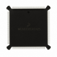
MC68332GVEH25 Freescale Semiconductor, MC68332GVEH25 Datasheet - Page 166

MC68332GVEH25
Manufacturer Part Number
MC68332GVEH25
Description
IC MCU 32BIT 25MHZ 132-PQFP
Manufacturer
Freescale Semiconductor
Series
M683xxr
Specifications of MC68332GVEH25
Core Processor
CPU32
Core Size
32-Bit
Speed
25MHz
Connectivity
EBI/EMI, SCI, SPI, UART/USART
Peripherals
POR, PWM, WDT
Number Of I /o
15
Program Memory Type
ROMless
Ram Size
2K x 8
Voltage - Supply (vcc/vdd)
4.5 V ~ 5.5 V
Oscillator Type
Internal
Operating Temperature
-40°C ~ 105°C
Package / Case
132-QFP
Processor Series
M683xx
Core
CPU32
Data Bus Width
32 bit
Controller Family/series
68K
No. Of I/o's
15
Ram Memory Size
2KB
Cpu Speed
25MHz
No. Of Timers
1
Embedded Interface Type
QSPI, SCI, UART
Digital Ic Case Style
PQFP
Rohs Compliant
Yes
Data Ram Size
2 KB
Interface Type
QSPI, SCI, UART
Maximum Clock Frequency
25 MHz
Number Of Programmable I/os
15
Number Of Timers
16
Maximum Operating Temperature
+ 105 C
Mounting Style
SMD/SMT
Minimum Operating Temperature
- 40 C
Lead Free Status / RoHS Status
Request inventory verification / Request inventory verification
Eeprom Size
-
Program Memory Size
-
Data Converters
-
Lead Free Status / Rohs Status
Lead free / RoHS Compliant
Available stocks
Company
Part Number
Manufacturer
Quantity
Price
Company:
Part Number:
MC68332GVEH25
Manufacturer:
Freescale Semiconductor
Quantity:
135
Company:
Part Number:
MC68332GVEH25
Manufacturer:
Freescale Semiconductor
Quantity:
10 000
- Current page: 166 of 265
- Download datasheet (7Mb)
7.6.1 System Configuration Registers
7.6.1.1 Prescaler Control for TCR1
7.6.1.2 Prescaler Control for TCR2
7-12
The TPU configuration control registers, TPUMCR and TICR, determine the value of
the prescaler, perform emulation control, specify whether the external TCR2 pin func-
tions as a clock source or as gate of the DIV8 clock for TCR2, and determine interrupt
request level and interrupt vector number assignment. Refer to APPENDIX D REGIS-
TER SUMMARY for more information about TPUMCR and TICR.
Timer control register one (TCR1) is clocked from the output of a prescaler. Two fields
in the TPUMCR control TCR1. The prescaler's input is the internal TPU system clock
divided by either 4 or 32, depending on the value of the PSCK (prescaler clock) bit.
The prescaler divides this input by 1, 2, 4, or 8, depending on the value of TCR1P (tim-
er count register 1 prescaler control). Channels using TCR1 have the capability to re-
solve down to the TPU system clock divided by 4. Refer to Figure 7-2 and Table 7-1.
Timer control register two (TCR2), like TCR1, is clocked from the output of a prescaler.
The T2CG (TCR2 clock/gate control) bit in TPUMCR determines whether the external
TCR2 pin functions as an external clock source for TCR2 or as the gate in the use of
TCR2 as a gated pulse accumulator. The function of the T2CG bit is shown in Figure
7-3.
SYSTEM
TCR1 Prescaler
CLOCK
00
01
10
11
32
Divide
4
By
Freescale Semiconductor, Inc.
1
2
4
8
For More Information On This Product,
Figure 7-2 TCR1 Prescaler Control
DIV32 CLOCK
Table 7-1 TCR1 Prescaler Control
DIV4 CLOCK
Go to: www.freescale.com
Number of
TIME PROCESSOR UNIT
Clocks
128
256
32
64
0 – DIV32
1 – DIV4
PSCK
MUX
PSCK = 0
16 MHz
Rate at
16 ms
2 ms
4 ms
8 ms
PRESCALER
00 1
01 2
10 4
11 8
TCR1
Number of
Clocks
16
32
4
8
PSCK = 1
0
USER’S MANUAL
TCR1
PRESCALER CTL BLOCK 1
16 MHz
Rate at
250 ns
500 ns
1 ms
2 ms
MC68332
15
Related parts for MC68332GVEH25
Image
Part Number
Description
Manufacturer
Datasheet
Request
R
Part Number:
Description:
Manufacturer:
Freescale Semiconductor, Inc
Datasheet:
Part Number:
Description:
Manufacturer:
Freescale Semiconductor, Inc
Datasheet:
Part Number:
Description:
Manufacturer:
Freescale Semiconductor, Inc
Datasheet:
Part Number:
Description:
Manufacturer:
Freescale Semiconductor, Inc
Datasheet:
Part Number:
Description:
Manufacturer:
Freescale Semiconductor, Inc
Datasheet:
Part Number:
Description:
Manufacturer:
Freescale Semiconductor, Inc
Datasheet:
Part Number:
Description:
Manufacturer:
Freescale Semiconductor, Inc
Datasheet:
Part Number:
Description:
Manufacturer:
Freescale Semiconductor, Inc
Datasheet:
Part Number:
Description:
Manufacturer:
Freescale Semiconductor, Inc
Datasheet:
Part Number:
Description:
Manufacturer:
Freescale Semiconductor, Inc
Datasheet:
Part Number:
Description:
Manufacturer:
Freescale Semiconductor, Inc
Datasheet:
Part Number:
Description:
Manufacturer:
Freescale Semiconductor, Inc
Datasheet:
Part Number:
Description:
Manufacturer:
Freescale Semiconductor, Inc
Datasheet:
Part Number:
Description:
Manufacturer:
Freescale Semiconductor, Inc
Datasheet:
Part Number:
Description:
Manufacturer:
Freescale Semiconductor, Inc
Datasheet:


