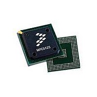
MPC5125YVN400 Freescale Semiconductor, MPC5125YVN400 Datasheet - Page 82

MPC5125YVN400
Manufacturer Part Number
MPC5125YVN400
Description
IC MCU 32BIT E300 324TEPBGA
Manufacturer
Freescale Semiconductor
Series
MPC51xxr
Datasheets
1.MPC5125YVN400.pdf
(92 pages)
2.MPC5125YVN400.pdf
(8 pages)
3.MPC5125YVN400.pdf
(2 pages)
4.MPC5125YVN400.pdf
(1064 pages)
Specifications of MPC5125YVN400
Core Processor
e300
Core Size
32-Bit
Speed
400MHz
Connectivity
CAN, EBI/EMI, Ethernet, I²C, USB OTG
Peripherals
DMA, WDT
Number Of I /o
64
Program Memory Type
ROMless
Ram Size
32K x 8
Voltage - Supply (vcc/vdd)
1.33 V ~ 1.47 V
Oscillator Type
External
Operating Temperature
-40°C ~ 125°C
Package / Case
324-PBGA
Processor Series
MPC51xx
Core
e300
Data Bus Width
32 bit
Development Tools By Supplier
TWR-MPC5125-KIT, TWR-SER, TWR-ELEV, TOWER
Maximum Clock Frequency
400 MHz
Operating Supply Voltage
1.4 V
Maximum Operating Temperature
+ 125 C
Mounting Style
SMD/SMT
Data Ram Size
32 KB
I/o Voltage
3.3 V
Interface Type
CAN, I2C
Minimum Operating Temperature
- 40 C
Program Memory Size
32 bit
Cpu Speed
400MHz
Embedded Interface Type
CAN, I2C, SPI, UART, USB
Digital Ic Case Style
TEPBGA
No. Of Pins
324
Rohs Compliant
Yes
Cpu Family
MPC5xx
Device Core Size
32b
Frequency (max)
400MHz
Total Internal Ram Size
32KB
Instruction Set Architecture
RISC
Operating Temp Range
-40C to 85C
Operating Temperature Classification
Industrial
Mounting
Surface Mount
Pin Count
324
Lead Free Status / RoHS Status
Lead free / RoHS Compliant
Eeprom Size
-
Program Memory Size
-
Data Converters
-
Lead Free Status / Rohs Status
Lead free / RoHS Compliant
Available stocks
Company
Part Number
Manufacturer
Quantity
Price
Company:
Part Number:
MPC5125YVN400
Manufacturer:
Freescale Semiconductor
Quantity:
135
Company:
Part Number:
MPC5125YVN400
Manufacturer:
LTC
Quantity:
29
Company:
Part Number:
MPC5125YVN400
Manufacturer:
Freescale Semiconductor
Quantity:
10 000
System Design Information
5
5.1
Power sequencing between the 1.4 V power supply V
during power-up phase.
The required power sequence is as follows:
5.2
Each of the independent PLL power supplies require filtering external to the device.
required filter circuit.
Each circuit should be placed as close as possible to the specific AV
nearby circuits.
All traces should be as low impedance as possible, especially ground pins to the ground plane.
The filter for system/core PLLVDD to V
planes.
In addition to keeping the filter components for system/core PLLVDD as close as practical to the body of the MPC5125 as
previously mentioned, special care should be taken to avoid coupling switching power supply noise or digital switching noise
onto the portion of that supply between the filter and the MPC5125.
The capacitors for C2 in the figure below should be rated X5R or better due to temperature performance. It is recommended to
add a bypass capacitance of at least 1 µF for the VBAT pin.
5.3
To ensure reliable operation, connect unused inputs to an appropriate signal level. Unused active low inputs should be tied to
V
Power and ground connections must be made to all external V
The unused AV
For DDR or LPDDR modes, the unused pins VTT[3:0] for DDR2 termination voltage can be unconnected.
82
DD_IO
•
•
•
•
•
. Unused active high inputs should be connected to V
Use 12 V/ms or slower time for all supplies.
Power up V
then power up V
All the supplies must reach the specified operating conditions before the PORESET can be released.
For power down, drop AV
V
power-up.
DD
System Design Information
Power Up/Down Sequencing
System and CPU Core AV
Connection Recommendations
should not exceed V
DD_FUSEWR
DD_IO
DD
Power supply
source
, AV
power should be connected to V
. If required AV
DD_PLL
DD_IO
DD_FUSEWR
s, V
MPC5125 Microcontroller Data Sheet, Rev. 3
SS
, V
C1= 1 µF
R1= 10 Ω
BAT
should be connected to the power and ground planes, respectively, not fingers of the
Figure 49. Power Supply Filtering
DD_IO_MEM
DD_FUSEWR
(if not applied permanently), and V
to 0 V first, drop V
DD
, V
should be powered up afterwards.
and the remaining supplies is required to prevent excessive current
DD
BAT
SS
SS
DD
, or AV
Power Supply Filtering
directly or via a resistor.
. All NC (no-connect) signals must remain unconnected.
and V
DD
DD
DD_PLL
to 0 V, and then drop all other supplies.
pin being supplied to minimize noise coupled from
SS
C2= 0.1 µF
pins of the MPC5125.
s by more than 0.4 V at any time, including
DD_IO_MEM
Figure 49
AV
DD
device pin
shows a recommendation for the
supplies first in any order, and
Freescale Semiconductor


