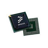
MPC5125YVN400 Freescale Semiconductor, MPC5125YVN400 Datasheet - Page 40

MPC5125YVN400
Manufacturer Part Number
MPC5125YVN400
Description
IC MCU 32BIT E300 324TEPBGA
Manufacturer
Freescale Semiconductor
Series
MPC51xxr
Datasheets
1.MPC5125YVN400.pdf
(92 pages)
2.MPC5125YVN400.pdf
(8 pages)
3.MPC5125YVN400.pdf
(2 pages)
4.MPC5125YVN400.pdf
(1064 pages)
Specifications of MPC5125YVN400
Core Processor
e300
Core Size
32-Bit
Speed
400MHz
Connectivity
CAN, EBI/EMI, Ethernet, I²C, USB OTG
Peripherals
DMA, WDT
Number Of I /o
64
Program Memory Type
ROMless
Ram Size
32K x 8
Voltage - Supply (vcc/vdd)
1.33 V ~ 1.47 V
Oscillator Type
External
Operating Temperature
-40°C ~ 125°C
Package / Case
324-PBGA
Processor Series
MPC51xx
Core
e300
Data Bus Width
32 bit
Development Tools By Supplier
TWR-MPC5125-KIT, TWR-SER, TWR-ELEV, TOWER
Maximum Clock Frequency
400 MHz
Operating Supply Voltage
1.4 V
Maximum Operating Temperature
+ 125 C
Mounting Style
SMD/SMT
Data Ram Size
32 KB
I/o Voltage
3.3 V
Interface Type
CAN, I2C
Minimum Operating Temperature
- 40 C
Program Memory Size
32 bit
Cpu Speed
400MHz
Embedded Interface Type
CAN, I2C, SPI, UART, USB
Digital Ic Case Style
TEPBGA
No. Of Pins
324
Rohs Compliant
Yes
Cpu Family
MPC5xx
Device Core Size
32b
Frequency (max)
400MHz
Total Internal Ram Size
32KB
Instruction Set Architecture
RISC
Operating Temp Range
-40C to 85C
Operating Temperature Classification
Industrial
Mounting
Surface Mount
Pin Count
324
Lead Free Status / RoHS Status
Lead free / RoHS Compliant
Eeprom Size
-
Program Memory Size
-
Data Converters
-
Lead Free Status / Rohs Status
Lead free / RoHS Compliant
Available stocks
Company
Part Number
Manufacturer
Quantity
Price
Company:
Part Number:
MPC5125YVN400
Manufacturer:
Freescale Semiconductor
Quantity:
135
Company:
Part Number:
MPC5125YVN400
Manufacturer:
LTC
Quantity:
29
Company:
Part Number:
MPC5125YVN400
Manufacturer:
Freescale Semiconductor
Quantity:
10 000
Electrical and Thermal Characteristics
NOTES:
1
NOTES:
1
2
3
4.1.4
40
General IO
Pad Type
Pad Type
1
V
V
General I/O—rise and fall times at drive load 50 pF.
DDR—rise and fall times at 50 Ω transmission line impedance terminated to MV
Rising slew rate measured between 0.5 × V
Falling slew rate measured between 0.5 × V
Sym
V
DDR
HBM
CDM
MM
Machine model (MM) — JEDEC JESD22-A115
Charge device model (CDM) — JEDEC JESD22-C101
Human body model (HBM) — JEDEC JESD22-A114-B
V
V
V
V
DD_IO_MEM
DD_IO_MEM
Electrostatic Discharge
DD_IO_MEM
DD_IO_MEM
This device contains circuitry that protects against damage due to high-static voltage or
electrical fields. However, it is advised that normal precautions be taken to avoid
application of any voltages higher than maximum-rated voltages. Operational
reliability is enhanced if unused inputs are tied to an appropriate logic voltage level (GND
or V
Supply Voltage
Supply Voltage
V
and SDR)
DD_IO
DD
= 1.8 V (LPDDR
= 1.8 V (DDR2) Configuration 2 (010)
).
= 2.5 V (DDR) Configuration 3 (011)
= 3.3 V (SDR) Configuration 7 (111)
Table 11
= 3.3 V
Table 7. General I/O Pads
Table 9. ESD and Latch-Up Protection Characteristics
Table 8. DDR I/O Pads
gives package thermal characteristics for this device.
MPC5125 Microcontroller Data Sheet, Rev. 3
Configuration 0 (000)
Configuration 1 (001)
Configuration 6 (110)
Slew Rate Control
Configuration 3 (11)
Configuration 2 (10)
Configuration 1 (01)
Configuration 0 (00)
Rating
Drive Select/Slew
DD_IO_MEM
DD_IO_MEM
Drive Select/
Rate Control
CAUTION
– 450 mV and 0.5 × V
+ 50 mV and 0.5 × V
1
— Drive Current, Slew Rate
1
— Drive Current, Slew Rate
Rising slew
max (ns)
Rise time
max (ns)
0.45
0.45
0.8
0.7
140
1.4
9.8
19
2
DD_IO_MEM
DD_IO_MEM
Falling slew
TT
max (ns)
max (ns)
Fall time
(0.5 × V
0.45
0.45
183
0.8
0.7
1.6
12
24
2000
– 450 mV for all modes.
Min
200
250
+ 50 mV for all modes.
3
DD_IO_MEM
Ioh (mA)
Current
Ioh (mA)
Current
16.2
13.4
35
4.6
8.1
5.3
Max
8
—
—
—
Freescale Semiconductor
) + 4 pF load.
Iol (mA)
Current
Current
Iol (mA)
Unit
16.2
13.4
35
4.6
8.1
5.3
V
V
V
8
SpecID
SpecID
SpecID
D3.41
D3.42
D3.43
D3.44
D3.45
D3.46
D3.47
D3.48
D3.49
D3.50
D4.1
D4.2
D4.3


