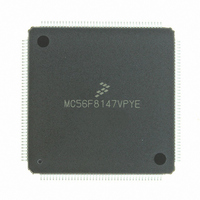
MC56F8147VPYE Freescale Semiconductor, MC56F8147VPYE Datasheet - Page 48

MC56F8147VPYE
Manufacturer Part Number
MC56F8147VPYE
Description
IC DSP 16BIT 40MHZ 160-LQFP
Manufacturer
Freescale Semiconductor
Series
56F8xxxr
Datasheet
1.MC56F8147VPYE.pdf
(172 pages)
Specifications of MC56F8147VPYE
Core Processor
56800
Core Size
16-Bit
Speed
40MHz
Connectivity
EBI/EMI, SCI, SPI
Peripherals
POR, PWM, WDT
Number Of I /o
76
Program Memory Size
128KB (64K x 16)
Program Memory Type
FLASH
Ram Size
4K x 16
Voltage - Supply (vcc/vdd)
2.25 V ~ 3.6 V
Data Converters
A/D 16x12b
Oscillator Type
External
Operating Temperature
-40°C ~ 105°C
Package / Case
160-LQFP
Data Bus Width
16 bit
Processor Series
MC56F81xx
Core
56800E
Data Ram Size
4 KB
Interface Type
SPI, SCI, CAN
Maximum Clock Frequency
40 MHz
Number Of Programmable I/os
76
Number Of Timers
2
Maximum Operating Temperature
+ 105 C
Mounting Style
SMD/SMT
Minimum Operating Temperature
- 40 C
On-chip Adc
4 x 12 bit, 4 Channel
Lead Free Status / RoHS Status
Lead free / RoHS Compliant
Eeprom Size
-
Lead Free Status / Rohs Status
Lead free / RoHS Compliant
Available stocks
Company
Part Number
Manufacturer
Quantity
Price
Company:
Part Number:
MC56F8147VPYE
Manufacturer:
FREESCAL
Quantity:
253
Company:
Part Number:
MC56F8147VPYE
Manufacturer:
Freescale Semiconductor
Quantity:
10 000
4.7 Peripheral Memory Mapped Registers
On-chip peripheral registers are part of the data memory map on the 56800E series. These locations may
be accessed with the same addressing modes used for ordinary Data memory, except all peripheral
registers should be read/written using word accesses only.
Table 4-9
Peripherals are listed in order of the base address.
The following tables list all of the peripheral registers required to control or access the peripherals.
Note: Features in italics are NOT available on the 56F8147 device.
48
External Memory Interface
Timer A
Timer B
Timer C
Timer D
PWM A
PWM B
Quadrature Decoder 0
Quadrature Decoder 1
ITCN
ADC A
ADC B
Temperature Sensor
SCI #0
SCI #1
SPI #0
SPI #1
COP
CLK, PLL, OSC, TEST
GPIO Port A
GPIO Port B
GPIO Port C
GPIO Port D
GPIO Port E
summarizes base addresses for the set of peripherals on the 56F8347 and 56F8147 devices.
Table 4-9 Data Memory Peripheral Base Address Map Summary
Peripheral
56F8347 Technical Data, Rev.11
EMI
TMRA
TMRB
TMRC
TMRD
PWMA
PWMB
DEC0
DEC1
ITCN
ADCA
ADCB
TSENSOR
SCI0
SCI1
SPI0
SPI1
COP
CLKGEN
GPIOA
GPIOB
GPIOC
GPIOD
GPIOE
Prefix
Base Address
X:$00 F0C0
X:$00 F1A0
X:$00 F2A0
X:$00 F2B0
X:$00 F2C0
X:$00 F2D0
X:$00 F2E0
X:$00 F020
X:$00 F040
X:$00 F080
X:$00 F100
X:$00 F140
X:$00 F160
X:$00 F180
X:$00 F190
X:$00 F200
X:$00 F240
X:$00 F270
X:$00 F280
X:$00 F290
X:$00 F300
X:$00 F310
X:$00 F320
X:$00 F330
Freescale Semiconductor
Table Number
4-10
4-11
4-12
4-13
4-14
4-15
4-16
4-17
4-18
4-19
4-20
4-21
4-22
4-23
4-24
4-25
4-26
4-27
4-28
4-29
4-30
4-31
4-32
4-33
Preliminary


