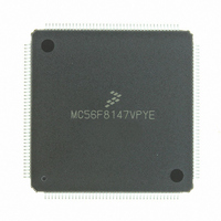
MC56F8147VPYE Freescale Semiconductor, MC56F8147VPYE Datasheet - Page 41

MC56F8147VPYE
Manufacturer Part Number
MC56F8147VPYE
Description
IC DSP 16BIT 40MHZ 160-LQFP
Manufacturer
Freescale Semiconductor
Series
56F8xxxr
Datasheet
1.MC56F8147VPYE.pdf
(172 pages)
Specifications of MC56F8147VPYE
Core Processor
56800
Core Size
16-Bit
Speed
40MHz
Connectivity
EBI/EMI, SCI, SPI
Peripherals
POR, PWM, WDT
Number Of I /o
76
Program Memory Size
128KB (64K x 16)
Program Memory Type
FLASH
Ram Size
4K x 16
Voltage - Supply (vcc/vdd)
2.25 V ~ 3.6 V
Data Converters
A/D 16x12b
Oscillator Type
External
Operating Temperature
-40°C ~ 105°C
Package / Case
160-LQFP
Data Bus Width
16 bit
Processor Series
MC56F81xx
Core
56800E
Data Ram Size
4 KB
Interface Type
SPI, SCI, CAN
Maximum Clock Frequency
40 MHz
Number Of Programmable I/os
76
Number Of Timers
2
Maximum Operating Temperature
+ 105 C
Mounting Style
SMD/SMT
Minimum Operating Temperature
- 40 C
On-chip Adc
4 x 12 bit, 4 Channel
Lead Free Status / RoHS Status
Lead free / RoHS Compliant
Eeprom Size
-
Lead Free Status / Rohs Status
Lead free / RoHS Compliant
Available stocks
Company
Part Number
Manufacturer
Quantity
Price
Company:
Part Number:
MC56F8147VPYE
Manufacturer:
FREESCAL
Quantity:
253
Company:
Part Number:
MC56F8147VPYE
Manufacturer:
Freescale Semiconductor
Quantity:
10 000
4.2 Program Map
The operating mode control bits (MA and MB) in the Operating Mode Register (OMR) control the
Program memory map. At reset, these bits are set as indicated in
map configurations that are possible at reset. After reset, the OMR MA bit can be changed and will have
an effect on the P-space memory map, as shown in
effect.
The device’s external memory interface (EMI) can operate much like the 56F80x family’s EMI, or it can
be operated in a mode similar to that used on other products in the 56800E family. Initially, CS0 and CS1
are configured as PS and DS, in a mode compatible with earlier 56800 devices.
Eighteen address lines are required to shadow the first 192K of internal program space when booting
externally for development purposes. Therefore, the entire complement of on-chip memory cannot be
accessed using a 16-bit 56800-compatible address bus. To address this situation, the EMI_MODE pin can
be used to configure four GPIO pins as Address[19:16] upon reset (Software reconfiguration of the highest
address lines [A20-23] is required if the full address range is to be used.)
The EMI_MODE pin also affects the reset vector address, as provided in
be configured as address or chip select signals to access addresses at P:$10 0000 and above.
Note: Program RAM is NOT available on the 56F8147 device.
Freescale Semiconductor
Preliminary
1. This bit is only configured at reset. If the Flash secured state changes, this will not be reflected in MB until the next reset.
2. Changing MB in software will not affect Flash memory security.
Flash Secured
OMR MB =
OMR MA
State
0
1
0
0
1
1
1, 2
Table 4-3 Changing OMR MA Value During Normal Operation
Use internal P-space memory map configuration
Use external P-space memory map configuration – If MB = 0 at reset, changing this bit has no effect.
EXTBOOT Pin
OMR MA =
0
1
0
1
Table 4-2 OMR MB/MA Value at Reset
Mode 0 – Internal Boot; EMI are configured to use 16 address lines; Flash Memory is
secured; external P-space is not allowed; the EOnCE is disabled
Not valid; cannot boot externally if the Flash is secured and will actually configure to
00 state
Mode 0 – Internal Boot; EMI is configured to use 16 address lines
Mode 1 – External Boot; Flash Memory is not secured; EMI configuration is
determined by the state of the EMI_MODE pin
56F8347 Technical Data, Rev.11
Chip Operating Mode
Table
Chip Operating Mode
4-3. Changing the OMR MB bit will have no
Table
4-2.
Table
Table 4-4
4-4. Additional pins must
shows the memory
Program Map
41


