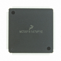
MC56F8147VPYE Freescale Semiconductor, MC56F8147VPYE Datasheet - Page 46

MC56F8147VPYE
Manufacturer Part Number
MC56F8147VPYE
Description
IC DSP 16BIT 40MHZ 160-LQFP
Manufacturer
Freescale Semiconductor
Series
56F8xxxr
Datasheet
1.MC56F8147VPYE.pdf
(172 pages)
Specifications of MC56F8147VPYE
Core Processor
56800
Core Size
16-Bit
Speed
40MHz
Connectivity
EBI/EMI, SCI, SPI
Peripherals
POR, PWM, WDT
Number Of I /o
76
Program Memory Size
128KB (64K x 16)
Program Memory Type
FLASH
Ram Size
4K x 16
Voltage - Supply (vcc/vdd)
2.25 V ~ 3.6 V
Data Converters
A/D 16x12b
Oscillator Type
External
Operating Temperature
-40°C ~ 105°C
Package / Case
160-LQFP
Data Bus Width
16 bit
Processor Series
MC56F81xx
Core
56800E
Data Ram Size
4 KB
Interface Type
SPI, SCI, CAN
Maximum Clock Frequency
40 MHz
Number Of Programmable I/os
76
Number Of Timers
2
Maximum Operating Temperature
+ 105 C
Mounting Style
SMD/SMT
Minimum Operating Temperature
- 40 C
On-chip Adc
4 x 12 bit, 4 Channel
Lead Free Status / RoHS Status
Lead free / RoHS Compliant
Eeprom Size
-
Lead Free Status / Rohs Status
Lead free / RoHS Compliant
Available stocks
Company
Part Number
Manufacturer
Quantity
Price
Company:
Part Number:
MC56F8147VPYE
Manufacturer:
FREESCAL
Quantity:
253
Company:
Part Number:
MC56F8147VPYE
Manufacturer:
Freescale Semiconductor
Quantity:
10 000
4.5 Flash Memory Map
Figure 4-1
The Flash Memory is divided into three functional blocks. The Program and boot memories reside on the
Program Memory buses. They are controlled by one set of banked registers. Data Memory Flash resides
on the Data Memory buses and is controlled separately by its own set of banked registers.
The top nine words of the Program Memory Flash are treated as special memory locations. The content of
these words is used to control the operation of the Flash Controller. Because these words are part of the
Flash Memory content, their state is maintained during power-down and reset. During chip initialization,
the content of these memory locations is loaded into Flash Memory control registers, detailed in the Flash
Memory chapter of the 56F8300 Peripheral User Manual. These configuration parameters are located
between $00_FFF7 and $00_FFFF.
Table 4-7
Note: Data Flash is NOT available on the 56F8147 device.
Please see 56F8300 Peripheral User Manual for additional Flash information.
46
PROG_FLASH_START + $00_FFFF
PROG_FLASH_START + $00_FFF7
PROG_FLASH_START + $00_FFF6
PROG_FLASH_START = $00_0000
BOOT_FLASH_START = $02_0000
Program Flash
BOOT_FLASH_START + $1FFF
Data Flash
Boot Flash
shows the page and sector sizes used within each Flash memory block on the chip.
illustrates the Flash Memory (FM) map on the system bus.
128K Bytes
Flash Size
Program Memory
128KB
Block 0 Even
Figure 4-1 Flash Array Memory Maps
Block 0 Odd
Table 4-7. Flash Memory Partitions
8KB
8KB
Configure Field
Reserved
Boot
8KB
56F8347 Technical Data, Rev.11
BLOCK 0 Odd (2 Bytes) $00_0003
BLOCK 0 Even (2 Bytes) $00_0002
BLOCK 0 Odd (2 Bytes) $00_0001
BLOCK 0 Even (2 Bytes) $00_0000
Sectors
FM_PROG_MEM_TOP = $00_FFFF
16
16
4
DATA_FLASH_START + $0FFF
DATA_FLASH_START + $0000
256 x 16 bits
Sector Size
4K x 16 bits
1K x 16 bits
FM_BASE + $14
FM_BASE + $00
Note: Data Flash is
NOT available in the
56F8147 device.
Unbanked Registers
Freescale Semiconductor
Data Memory
Banked Registers
512 x 16 bits
256 x 16 bits
256 x 16 bits
Page Size
8KB
Preliminary


