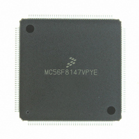
MC56F8147VPYE Freescale Semiconductor, MC56F8147VPYE Datasheet - Page 24

MC56F8147VPYE
Manufacturer Part Number
MC56F8147VPYE
Description
IC DSP 16BIT 40MHZ 160-LQFP
Manufacturer
Freescale Semiconductor
Series
56F8xxxr
Datasheet
1.MC56F8147VPYE.pdf
(172 pages)
Specifications of MC56F8147VPYE
Core Processor
56800
Core Size
16-Bit
Speed
40MHz
Connectivity
EBI/EMI, SCI, SPI
Peripherals
POR, PWM, WDT
Number Of I /o
76
Program Memory Size
128KB (64K x 16)
Program Memory Type
FLASH
Ram Size
4K x 16
Voltage - Supply (vcc/vdd)
2.25 V ~ 3.6 V
Data Converters
A/D 16x12b
Oscillator Type
External
Operating Temperature
-40°C ~ 105°C
Package / Case
160-LQFP
Data Bus Width
16 bit
Processor Series
MC56F81xx
Core
56800E
Data Ram Size
4 KB
Interface Type
SPI, SCI, CAN
Maximum Clock Frequency
40 MHz
Number Of Programmable I/os
76
Number Of Timers
2
Maximum Operating Temperature
+ 105 C
Mounting Style
SMD/SMT
Minimum Operating Temperature
- 40 C
On-chip Adc
4 x 12 bit, 4 Channel
Lead Free Status / RoHS Status
Lead free / RoHS Compliant
Eeprom Size
-
Lead Free Status / Rohs Status
Lead free / RoHS Compliant
Available stocks
Company
Part Number
Manufacturer
Quantity
Price
Company:
Part Number:
MC56F8147VPYE
Manufacturer:
FREESCAL
Quantity:
253
Company:
Part Number:
MC56F8147VPYE
Manufacturer:
Freescale Semiconductor
Quantity:
10 000
24
Table 2-2 Signal and Package Information for the 160-Pin LQFP and MBGA (Continued)
Signal Name
(GPIOF0)
(GPIOF1)
(GPIOF2)
(GPIOF3)
(GPIOF4)
(GPIOF5)
(GPIOF6)
(GPIOF7)
(GPIOF8)
D10
D11
D12
D13
D14
D15
RD
D7
D8
D9
149
150
151
152
153
Pin
No.
28
29
30
32
52
Ball
No.
C4
K1
K3
K2
K4
A5
A4
B5
A3
P5
Output
Output
Output
Input/
Input/
Type
56F8347 Technical Data, Rev.11
disabled,
pull-up is
disabled,
pull-up is
output is
output is
In reset,
enabled
In reset,
enabled
During
Reset
State
Read Enable — RD is asserted during external memory
read cycles. When RD is asserted low, pins D0 - D15
become inputs and an external device is enabled onto the
data bus. When RD is deasserted high, the external data is
latched inside the device. When RD is asserted, it qualifies
the A0 - A16, PS, and DS pins. RD can be connected directly
to the OE pin of a static RAM or ROM.
Depending upon the state of the DRV bit in the EMI bus control
register (BCR), RD is tri-stated when the external bus is
inactive.
Most designs will want to change the DRV state to DRV = 1
instead of using the default setting.
To deactivate the internal pull-up resistor, set the CTRL bit in
the SIM_PUDR register.
Data Bus — D7 - D15 specify part of the data for external
program or data memory accesses.
Depending upon the state of the DRV bit in the EMI bus
control register (BCR), D7 - D15 are tri-stated when the
external bus is inactive.
Most designs will want to change the DRV state to DRV = 1
instead of using the default setting.
Port F GPIO — These nine GPIO pins can be individually
programmed as input or output pins.
At reset, these pins default to data bus functionality.
To deactivate the internal pull-up resistor, clear the
appropriate GPIO bit in the GPIOF_PUR register.
Example: GPIOF0, clear bit 0 in the GPIOF_PUR register.
Signal Description
Freescale Semiconductor
Preliminary


