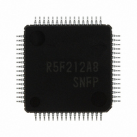
R5F212A8SNFP#U0 Renesas Electronics America, R5F212A8SNFP#U0 Datasheet - Page 516

R5F212A8SNFP#U0
Manufacturer Part Number
R5F212A8SNFP#U0
Description
IC R8C/2A MCU FLASH 64LQFP
Manufacturer
Renesas Electronics America
Series
R8C/2x/2Ar
Specifications of R5F212A8SNFP#U0
Core Processor
R8C
Core Size
16/32-Bit
Speed
20MHz
Connectivity
I²C, LIN, SIO, SSU, UART/USART
Peripherals
POR, PWM, Voltage Detect, WDT
Number Of I /o
55
Program Memory Size
64KB (64K x 8)
Program Memory Type
FLASH
Ram Size
3K x 8
Voltage - Supply (vcc/vdd)
2.2 V ~ 5.5 V
Data Converters
A/D 12x10b; D/A 2x8b
Oscillator Type
Internal
Operating Temperature
-20°C ~ 85°C
Package / Case
64-LQFP
For Use With
R0K5212D8S001BE - KIT STARTER FOR R8C/2DR0K5212D8S000BE - KIT DEV FOR R8C/2D
Lead Free Status / RoHS Status
Lead free / RoHS Compliant
Eeprom Size
-
Available stocks
Company
Part Number
Manufacturer
Quantity
Price
- Current page: 516 of 611
- Download datasheet (7Mb)
R8C/2A Group, R8C/2B Group
Rev.2.00
REJ09B0324-0200
20.4
Table 20.3
NOTE:
Operating mode
Areas in which a rewrite
control program can be
located
Areas in which a rewrite
control program can be
executed
Areas which can be
rewritten
Software command
restrictions
Modes after program or
erase
Modes after read status
register
CPU status during auto-
write and auto-erase
Flash memory status
detection
Conditions for transition to
erase-suspend
Conditions for transitions to
program-suspend
CPU clock
In CPU rewrite mode, the user ROM area can be rewritten by executing software commands from the CPU.
Therefore, the user ROM area can be rewritten directly while the MCU is mounted on a board without using a
ROM programmer. Execute the program and block erase commands only to blocks in the user ROM area.
The flash module has an erase-suspend function when an interrupt request is generated during an erase operation in
CPU rewrite mode. It performs an interrupt process after the erase operation is halted temporarily. During erase-
suspend, the user ROM area can be read by a program.
In case an interrupt request is generated during an auto-program operation in CPU rewrite mode, the flash module
has a program-suspend function which performs the interrupt process after the auto-program operation is
suspended. During program-suspend, the user ROM area can be read by a program.
CPU rewrite mode has an erase write 0 mode (EW0 mode) and an erase write 1 mode (EW1 mode). Table 20.3 lists
the Differences between EW0 Mode and EW1 Mode.
1. When the FMR02 bit in the FMR0 register is set to 1 (rewrite enabled), rewriting block 0 is enabled by setting
the FMR15 bit in the FMR1 register to 0 (rewrite enabled), and rewriting block 1 is enabled by setting the
FMR16 bit to 0 (rewrite enabled).
When the FMR02 bit in the FMR0 register is set to 1 (rewrite enabled), blocks 2 and 3 are rewritable.
CPU Rewrite Mode
Nov 26, 2007
Item
Differences between EW0 Mode and EW1 Mode
Page 494 of 580
User ROM area
Necessary to transfer to any area other
than the flash memory (e.g., RAM) before
executing
User ROM area
None
Read status register mode
Read status register mode
Operating
• Read bits FMR00, FMR06, and FMR07
• Execute the read status register
Set bits FMR40 and FMR41 in the FMR4
register to 1 by a program.
Set bits FMR40 and FMR42 in the FMR4
register to 1 by a program.
Single-chip mode
5 MHz or below
in the FMR0 register by a program
command and read bits SR7, SR5, and
SR4 in the status register.
EW0 Mode
Single-chip mode
User ROM area
Executing directly in user ROM or RAM
area possible
User ROM area
• Program and block erase commands
• Read status register command
Read array mode
Do not execute this command
Hold state (I/O ports hold state before the
command is executed)
Read bits FMR00, FMR06, and FMR07 in
the FMR0 register by a program
The FMR40 bit in the FMR4 register is set
to 1 and the interrupt request of the
enabled maskable interrupt is generated
The FMR40 bit in the FMR4 register is set
to 1 and the interrupt request of the
enabled maskable interrupt is generated
No restriction (on clock frequency to be
used)
Cannot be run on any block which
contains a rewrite control program
Cannot be executed
However, blocks which contain a rewrite
control program are excluded
EW1 Mode
20. Flash Memory
(1)
Related parts for R5F212A8SNFP#U0
Image
Part Number
Description
Manufacturer
Datasheet
Request
R

Part Number:
Description:
KIT STARTER FOR M16C/29
Manufacturer:
Renesas Electronics America
Datasheet:

Part Number:
Description:
KIT STARTER FOR R8C/2D
Manufacturer:
Renesas Electronics America
Datasheet:

Part Number:
Description:
R0K33062P STARTER KIT
Manufacturer:
Renesas Electronics America
Datasheet:

Part Number:
Description:
KIT STARTER FOR R8C/23 E8A
Manufacturer:
Renesas Electronics America
Datasheet:

Part Number:
Description:
KIT STARTER FOR R8C/25
Manufacturer:
Renesas Electronics America
Datasheet:

Part Number:
Description:
KIT STARTER H8S2456 SHARPE DSPLY
Manufacturer:
Renesas Electronics America
Datasheet:

Part Number:
Description:
KIT STARTER FOR R8C38C
Manufacturer:
Renesas Electronics America
Datasheet:

Part Number:
Description:
KIT STARTER FOR R8C35C
Manufacturer:
Renesas Electronics America
Datasheet:

Part Number:
Description:
KIT STARTER FOR R8CL3AC+LCD APPS
Manufacturer:
Renesas Electronics America
Datasheet:

Part Number:
Description:
KIT STARTER FOR RX610
Manufacturer:
Renesas Electronics America
Datasheet:

Part Number:
Description:
KIT STARTER FOR R32C/118
Manufacturer:
Renesas Electronics America
Datasheet:

Part Number:
Description:
KIT DEV RSK-R8C/26-29
Manufacturer:
Renesas Electronics America
Datasheet:

Part Number:
Description:
KIT STARTER FOR SH7124
Manufacturer:
Renesas Electronics America
Datasheet:

Part Number:
Description:
KIT STARTER FOR H8SX/1622
Manufacturer:
Renesas Electronics America
Datasheet:

Part Number:
Description:
KIT DEV FOR SH7203
Manufacturer:
Renesas Electronics America
Datasheet:


