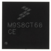
MC9S08LC36LH Freescale Semiconductor, MC9S08LC36LH Datasheet - Page 81

MC9S08LC36LH
Manufacturer Part Number
MC9S08LC36LH
Description
IC MCU 36K FLASH 2K RAM 64-LQFP
Manufacturer
Freescale Semiconductor
Series
HCS08r
Specifications of MC9S08LC36LH
Core Processor
HCS08
Core Size
8-Bit
Speed
40MHz
Connectivity
I²C, SCI, SPI
Peripherals
LCD, LVD, POR, PWM, WDT
Number Of I /o
18
Program Memory Size
36KB (36K x 8)
Program Memory Type
FLASH
Ram Size
2.5K x 8
Voltage - Supply (vcc/vdd)
1.8 V ~ 3.6 V
Data Converters
A/D 2x12b
Oscillator Type
External
Operating Temperature
0°C ~ 70°C
Package / Case
64-LQFP
Processor Series
S08LC
Core
HCS08
Data Bus Width
8 bit
Data Ram Size
2.5 KB
Interface Type
I2C/SCI/SPI1/SPI2
Maximum Clock Frequency
40 MHz
Number Of Programmable I/os
18
Maximum Operating Temperature
+ 85 C
Mounting Style
SMD/SMT
3rd Party Development Tools
EWS08
Minimum Operating Temperature
- 40 C
On-chip Adc
2-ch x 12-bit
For Use With
DEMO9S08LC60 - BOARD DEMO FOR 9S08LC60
Lead Free Status / RoHS Status
Lead free / RoHS Compliant
Eeprom Size
-
Lead Free Status / Rohs Status
Lead free / RoHS Compliant
Available stocks
Company
Part Number
Manufacturer
Quantity
Price
Company:
Part Number:
MC9S08LC36LH
Manufacturer:
Freescale Semiconductor
Quantity:
10 000
- Current page: 81 of 360
- Download datasheet (4Mb)
Chapter 6
Parallel Input/Output
This section explains software controls related to parallel input/output (I/O). The MC9S08LC60 Series has
three I/O ports which include a total of up to 24 general-purpose I/O pins (pin availability depends on
device and package option, see
information about the logic and hardware aspects of these pins.
Many of these pins are shared with on-chip peripherals such as timer systems, SPI, SCI, IIC, external
interrupts, or keyboard interrupts as shown in Table 2-1. The peripheral modules have priority over the I/Os
so that when a peripheral is enabled, the I/O functions associated with the shared pins are disabled. After
reset, the shared peripheral functions are disabled so that the pins are controlled by the I/O. All of the I/Os
are configured as inputs (PTxDDn = 0) with pullup devices disabled (PTxPEn = 0), except for output-only
pin PTC6 which defaults to BKGD/MS pin and PTB2 which defaults to the RESET function.
When these other modules are not controlling the port pins, they revert to general-purpose I/O control. As
a general-purpose I/O control, a port data bit provides access to input (read) and output (write) data, a data
direction bit controls the direction of the pin, and a pullup enable bit enables an internal pullup device
(provided the pin is configured as an input), and a slew rate control bit controls the rise and fall times of
the pins.
Reading and writing of parallel I/Os is performed through the port data registers. The direction, either input
or output, is controlled through the port data direction registers. The parallel I/O port function for an
individual pin is illustrated in the block diagram shown in
Freescale Semiconductor
Not all general-purpose I/O pins are available on all packages. To avoid
extra current drain from floating input pins, the user’s reset initialization
routine in the application program should either enable on-chip pullup
devices or change the direction of unconnected pins to outputs so the pins
do not float.
MC9S08LC60 Series Data Sheet: Technical Data, Rev. 4
Table 1-2
for details). See
NOTE
Chapter 2, “Pins and
Figure
6-1.
Connections,” for more
81
Related parts for MC9S08LC36LH
Image
Part Number
Description
Manufacturer
Datasheet
Request
R
Part Number:
Description:
Manufacturer:
Freescale Semiconductor, Inc
Datasheet:
Part Number:
Description:
Manufacturer:
Freescale Semiconductor, Inc
Datasheet:
Part Number:
Description:
Manufacturer:
Freescale Semiconductor, Inc
Datasheet:
Part Number:
Description:
Manufacturer:
Freescale Semiconductor, Inc
Datasheet:
Part Number:
Description:
Manufacturer:
Freescale Semiconductor, Inc
Datasheet:
Part Number:
Description:
Manufacturer:
Freescale Semiconductor, Inc
Datasheet:
Part Number:
Description:
Manufacturer:
Freescale Semiconductor, Inc
Datasheet:
Part Number:
Description:
Manufacturer:
Freescale Semiconductor, Inc
Datasheet:
Part Number:
Description:
Manufacturer:
Freescale Semiconductor, Inc
Datasheet:
Part Number:
Description:
Manufacturer:
Freescale Semiconductor, Inc
Datasheet:
Part Number:
Description:
Manufacturer:
Freescale Semiconductor, Inc
Datasheet:
Part Number:
Description:
Manufacturer:
Freescale Semiconductor, Inc
Datasheet:
Part Number:
Description:
Manufacturer:
Freescale Semiconductor, Inc
Datasheet:
Part Number:
Description:
Manufacturer:
Freescale Semiconductor, Inc
Datasheet:
Part Number:
Description:
Manufacturer:
Freescale Semiconductor, Inc
Datasheet:


