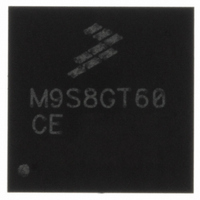
MC9S08LC36LH Freescale Semiconductor, MC9S08LC36LH Datasheet - Page 128

MC9S08LC36LH
Manufacturer Part Number
MC9S08LC36LH
Description
IC MCU 36K FLASH 2K RAM 64-LQFP
Manufacturer
Freescale Semiconductor
Series
HCS08r
Specifications of MC9S08LC36LH
Core Processor
HCS08
Core Size
8-Bit
Speed
40MHz
Connectivity
I²C, SCI, SPI
Peripherals
LCD, LVD, POR, PWM, WDT
Number Of I /o
18
Program Memory Size
36KB (36K x 8)
Program Memory Type
FLASH
Ram Size
2.5K x 8
Voltage - Supply (vcc/vdd)
1.8 V ~ 3.6 V
Data Converters
A/D 2x12b
Oscillator Type
External
Operating Temperature
0°C ~ 70°C
Package / Case
64-LQFP
Processor Series
S08LC
Core
HCS08
Data Bus Width
8 bit
Data Ram Size
2.5 KB
Interface Type
I2C/SCI/SPI1/SPI2
Maximum Clock Frequency
40 MHz
Number Of Programmable I/os
18
Maximum Operating Temperature
+ 85 C
Mounting Style
SMD/SMT
3rd Party Development Tools
EWS08
Minimum Operating Temperature
- 40 C
On-chip Adc
2-ch x 12-bit
For Use With
DEMO9S08LC60 - BOARD DEMO FOR 9S08LC60
Lead Free Status / RoHS Status
Lead free / RoHS Compliant
Eeprom Size
-
Lead Free Status / Rohs Status
Lead free / RoHS Compliant
Available stocks
Company
Part Number
Manufacturer
Quantity
Price
Company:
Part Number:
MC9S08LC36LH
Manufacturer:
Freescale Semiconductor
Quantity:
10 000
- Current page: 128 of 360
- Download datasheet (4Mb)
Chapter 9 Liquid Crystal Display Driver (S08LCDV1)
9.2.6
The charge pump capacitor is used to transfer charge from the input supply to the regulated output. It is
recommended that a low equivalent series resistance (ESR) capacitor be used. Proper orientation is
imperative when using a polarized capacitor.
9.3
This section consists of register descriptions. Each description includes a standard register diagram.
Details of register bit and field function follow the register diagrams, in bit order.
9.3.1
Read: anytime
Write: LCDEN anytime. To avoid segment flicker the clock prescaler bits (LCLK[2:0]) and the duty select
bits (DUTY[1:0]) must not be changed when the LCD module is enabled.
128
LPWAVE
Reset
LCDEN
Field
7
6
W
R
Register Definition
LCDEN
V
LCD Control Register 0 (LCDCR0)
LCD Driver Enable — The LCDEN bit starts the LCD module waveform generator.
0 All frontplane and backplane pins are disabled. In addition, the LCD module system is disabled and all LCD
1 LCD module driver system is enabled. All frontplanes pins enabled using the frontplane enable register will
LCD Waveform — The LPWAVE bit allows selection of two types of LCD waveforms.
0 Normal waveforms selected.
1 Low-power waveforms selected.
0
7
cap1
waveform generation clocks are stopped.
output an LCD module driver waveform.The backplane pins will output an LCD module driver waveform
based on the settings of DUTY0 and DUTY1.
, V
= Unimplemented or Reserved
LPWAVE
cap2
1
6
MC9S08LC60 Series Data Sheet: Technical Data, Rev. 4
Figure 9-3. LCD Control Register 0 (LCDCR0)
Table 9-4. LCDCR0 Field Descriptions
LCLK2
0
5
LCLK1
0
4
Description
LCLK0
3
0
0
0
2
Freescale Semiconductor
DUTY1
1
1
DUTY0
1
0
Related parts for MC9S08LC36LH
Image
Part Number
Description
Manufacturer
Datasheet
Request
R
Part Number:
Description:
Manufacturer:
Freescale Semiconductor, Inc
Datasheet:
Part Number:
Description:
Manufacturer:
Freescale Semiconductor, Inc
Datasheet:
Part Number:
Description:
Manufacturer:
Freescale Semiconductor, Inc
Datasheet:
Part Number:
Description:
Manufacturer:
Freescale Semiconductor, Inc
Datasheet:
Part Number:
Description:
Manufacturer:
Freescale Semiconductor, Inc
Datasheet:
Part Number:
Description:
Manufacturer:
Freescale Semiconductor, Inc
Datasheet:
Part Number:
Description:
Manufacturer:
Freescale Semiconductor, Inc
Datasheet:
Part Number:
Description:
Manufacturer:
Freescale Semiconductor, Inc
Datasheet:
Part Number:
Description:
Manufacturer:
Freescale Semiconductor, Inc
Datasheet:
Part Number:
Description:
Manufacturer:
Freescale Semiconductor, Inc
Datasheet:
Part Number:
Description:
Manufacturer:
Freescale Semiconductor, Inc
Datasheet:
Part Number:
Description:
Manufacturer:
Freescale Semiconductor, Inc
Datasheet:
Part Number:
Description:
Manufacturer:
Freescale Semiconductor, Inc
Datasheet:
Part Number:
Description:
Manufacturer:
Freescale Semiconductor, Inc
Datasheet:
Part Number:
Description:
Manufacturer:
Freescale Semiconductor, Inc
Datasheet:


