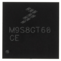
MC9S08LC36LH Freescale Semiconductor, MC9S08LC36LH Datasheet - Page 129

MC9S08LC36LH
Manufacturer Part Number
MC9S08LC36LH
Description
IC MCU 36K FLASH 2K RAM 64-LQFP
Manufacturer
Freescale Semiconductor
Series
HCS08r
Specifications of MC9S08LC36LH
Core Processor
HCS08
Core Size
8-Bit
Speed
40MHz
Connectivity
I²C, SCI, SPI
Peripherals
LCD, LVD, POR, PWM, WDT
Number Of I /o
18
Program Memory Size
36KB (36K x 8)
Program Memory Type
FLASH
Ram Size
2.5K x 8
Voltage - Supply (vcc/vdd)
1.8 V ~ 3.6 V
Data Converters
A/D 2x12b
Oscillator Type
External
Operating Temperature
0°C ~ 70°C
Package / Case
64-LQFP
Processor Series
S08LC
Core
HCS08
Data Bus Width
8 bit
Data Ram Size
2.5 KB
Interface Type
I2C/SCI/SPI1/SPI2
Maximum Clock Frequency
40 MHz
Number Of Programmable I/os
18
Maximum Operating Temperature
+ 85 C
Mounting Style
SMD/SMT
3rd Party Development Tools
EWS08
Minimum Operating Temperature
- 40 C
On-chip Adc
2-ch x 12-bit
For Use With
DEMO9S08LC60 - BOARD DEMO FOR 9S08LC60
Lead Free Status / RoHS Status
Lead free / RoHS Compliant
Eeprom Size
-
Lead Free Status / Rohs Status
Lead free / RoHS Compliant
Available stocks
Company
Part Number
Manufacturer
Quantity
Price
Company:
Part Number:
MC9S08LC36LH
Manufacturer:
Freescale Semiconductor
Quantity:
10 000
- Current page: 129 of 360
- Download datasheet (4Mb)
9.3.2
Read: anytime
Freescale Semiconductor
DUTY[1:0]
LCLK[2:0]
LCDSTP3
LCDWAI
LCDIEN
Reset
Field
Field
5:3
1:0
7
1
0
W
R
LCDIEN
LCD Control Register 1 (LCDCR1)
LCD Clock Prescaler — The LCD module clock prescaler bits are used as a clock divider to generate the LCD
waveform base clock as shown in
cycle configuration to determine the LCD module frame frequency.LCD module frame frequency calculations are
provided in 9.4.1.3/p.139.
LCD Duty Select — DUTY[1:0] bits select the duty cycle of the LCD module driver.
00 Reserved.
01 Use BP[1:0] (1/2 duty cycle). This mode forces the multiplexed BP3/FP40 pin to be configured as FP40
10 Use BP[2:0] (1/3 duty cycle). This mode forces the multiplexed BP3/FP40 pin to be configured as FP40
11 Use BP[3:0] (1/4 duty cycle). This mode forces the multiplexed BP3/FP40 pin to be configured as BP3
LCD Module Frame Frequency Interrupt Enable — Enables an LCD interrupt.event that coincides with the
LCD module frame frequency (LPWAVE=0) or sub-frame frequency (LPWAVE=1).
0 The start of the LCD module frame causes a LCD module interrupt request.
1 No Interrupt request is generated by this event.
LCD Module Driver and Charge Pump Stop While in Wait Mode
0 Allows the LCD driver and charge pump to continue running during wait mode.
1 Disables the LCD driver and charge pump whenever the MCU goes into wait mode.
LCD Module Driver and Charge Pump Stop While in Stop3 Mode
0 Allows the LCD module driver and charge pump to continue running during stop3.
1 Disables the LCD module driver and charge pump whenever the MCU goes into stop3.
0
7
(default)
LCD Waveform Base Clock
= Unimplemented or Reserved
0
0
6
Table 9-4. LCDCR0 Field Descriptions (continued)
MC9S08LC60 Series Data Sheet: Technical Data, Rev. 4
Figure 9-4. LCD Control Register 1 (LCDCR1)
Table 9-5. LCDCR1 Field Descriptions
0
0
5
Equation
=
9-1. The waveform base clock is used, with the LCD module duty
16 x 2
0
0
4
LCDCLK
Description
Description
LCLK[2:0]
3
0
0
Chapter 9 Liquid Crystal Display Driver (S08LCDV1)
0
0
2
where LCDCLK ≅ 32.768 kHz
LCDWAI
0
1
LCDSTP3
Eqn. 9-1
0
0
129
Related parts for MC9S08LC36LH
Image
Part Number
Description
Manufacturer
Datasheet
Request
R
Part Number:
Description:
Manufacturer:
Freescale Semiconductor, Inc
Datasheet:
Part Number:
Description:
Manufacturer:
Freescale Semiconductor, Inc
Datasheet:
Part Number:
Description:
Manufacturer:
Freescale Semiconductor, Inc
Datasheet:
Part Number:
Description:
Manufacturer:
Freescale Semiconductor, Inc
Datasheet:
Part Number:
Description:
Manufacturer:
Freescale Semiconductor, Inc
Datasheet:
Part Number:
Description:
Manufacturer:
Freescale Semiconductor, Inc
Datasheet:
Part Number:
Description:
Manufacturer:
Freescale Semiconductor, Inc
Datasheet:
Part Number:
Description:
Manufacturer:
Freescale Semiconductor, Inc
Datasheet:
Part Number:
Description:
Manufacturer:
Freescale Semiconductor, Inc
Datasheet:
Part Number:
Description:
Manufacturer:
Freescale Semiconductor, Inc
Datasheet:
Part Number:
Description:
Manufacturer:
Freescale Semiconductor, Inc
Datasheet:
Part Number:
Description:
Manufacturer:
Freescale Semiconductor, Inc
Datasheet:
Part Number:
Description:
Manufacturer:
Freescale Semiconductor, Inc
Datasheet:
Part Number:
Description:
Manufacturer:
Freescale Semiconductor, Inc
Datasheet:
Part Number:
Description:
Manufacturer:
Freescale Semiconductor, Inc
Datasheet:


