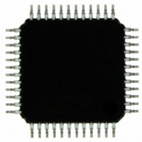
C8051F501-IQ Silicon Laboratories Inc, C8051F501-IQ Datasheet - Page 248

C8051F501-IQ
Manufacturer Part Number
C8051F501-IQ
Description
IC 8051 MCU 64K FLASH 48-QFP
Manufacturer
Silicon Laboratories Inc
Series
C8051F50xr
Specifications of C8051F501-IQ
Program Memory Type
FLASH
Program Memory Size
64KB (64K x 8)
Package / Case
48-QFP
Mfg Application Notes
LIN Bootloader AppNote
Core Processor
8051
Core Size
8-Bit
Speed
50MHz
Connectivity
EBI/EMI, SMBus (2-Wire/I²C), SPI, UART/USART
Peripherals
POR, PWM, Temp Sensor, WDT
Number Of I /o
40
Ram Size
4.25K x 8
Voltage - Supply (vcc/vdd)
1.8 V ~ 5.25 V
Data Converters
A/D 32x12b
Oscillator Type
Internal
Operating Temperature
-40°C ~ 125°C
Processor Series
C8051F5x
Core
8051
Data Bus Width
8 bit
Data Ram Size
4.25 KB
Interface Type
I2C/SPI/UART
Maximum Clock Frequency
50 MHz
Number Of Programmable I/os
40
Number Of Timers
4
Maximum Operating Temperature
+ 125 C
Mounting Style
SMD/SMT
3rd Party Development Tools
PK51, CA51, A51, ULINK2
Development Tools By Supplier
C8051F500DK
Minimum Operating Temperature
- 40 C
On-chip Adc
32-ch x 12-bit
Package
48PQFP
Device Core
8051
Family Name
C8051F50x
Maximum Speed
50 MHz
Operating Supply Voltage
2.5|3.3|5 V
Lead Free Status / RoHS Status
Lead free / RoHS Compliant
For Use With
336-1527 - KIT DEV FOR C8051F50X
Eeprom Size
-
Lead Free Status / Rohs Status
Lead free / RoHS Compliant
Other names
336-1512
Available stocks
Company
Part Number
Manufacturer
Quantity
Price
Company:
Part Number:
C8051F501-IQ
Manufacturer:
Silicon Laboratories Inc
Quantity:
10 000
Company:
Part Number:
C8051F501-IQR
Manufacturer:
Silicon Laboratories Inc
Quantity:
10 000
- Current page: 248 of 312
- Download datasheet (3Mb)
C8051F50x/F51x
SFR Definition 24.1. SCON0: Serial Port 0 Control
SFR Address = 0x98; Bit-Addressable; SFR Page = 0x00
248
Name
Reset
Bit
Type
7
6
5
4
3
2
1
0
Bit
PERR0
THRE0
Name
OVR0
REN0
RBX0
TBX0
RI0
TI0
OVR0
R/W
7
0
Receive FIFO Overrun Flag.
0: Receive FIFO Overrun has not occurred
1: Receive FIFO Overrun has occurred; A received character has been discarded due
to a full FIFO.
Parity Error Flag.
When parity is enabled, this bit indicates that a parity error has occurred. It is set to 1
when the parity of the oldest byte in the FIFO does not match the selected Parity Type.
0: Parity error has not occurred
1: Parity error has occurred.
This bit must be cleared by software.
Transmit Holding Register Empty Flag.
0: Transmit Holding Register not Empty—do not write to SBUF0.
1: Transmit Holding Register Empty—it is safe to write to SBUF0.
Receive Enable.
This bit enables/disables the UART receiver. When disabled, bytes can still be read
from the receive FIFO.
0: UART1 reception disabled.
1: UART1 reception enabled.
Extra Transmission Bit.
The logic level of this bit will be assigned to the extra transmission bit when XBE0 is set
to 1. This bit is not used when Parity is enabled.
Extra Receive Bit.
RBX0 is assigned the value of the extra bit when XBE1 is set to 1. If XBE1 is cleared to
0, RBX1 will be assigned the logic level of the first stop bit. This bit is not valid when
Parity is enabled.
Transmit Interrupt Flag.
Set to a 1 by hardware after data has been transmitted, at the beginning of the STOP
bit. When the UART0 interrupt is enabled, setting this bit causes the CPU to vector to
the UART0 interrupt service routine. This bit must be cleared manually by software.
Receive Interrupt Flag.
Set to 1 by hardware when a byte of data has been received by UART0 (set at the
STOP bit sampling time). When the UART0 interrupt is enabled, setting this bit to 1
causes the CPU to vector to the UART0 interrupt service routine. This bit must be
cleared manually by software. Note that RI0 will remain set to ‘1’ as long as there is
data still in the UART FIFO. After the last byte has been shifted from the FIFO to
SBUF0, RI0 can be cleared.
PERR0
R/W
6
0
THRE0
R
5
1
REN0
R/W
Rev. 1.2
4
0
Function
TBX0
R/W
3
0
RBX0
R/W
2
0
R/W
TI0
1
0
R/W
RI0
0
0
Related parts for C8051F501-IQ
Image
Part Number
Description
Manufacturer
Datasheet
Request
R
Part Number:
Description:
SMD/C°/SINGLE-ENDED OUTPUT SILICON OSCILLATOR
Manufacturer:
Silicon Laboratories Inc
Part Number:
Description:
Manufacturer:
Silicon Laboratories Inc
Datasheet:
Part Number:
Description:
N/A N/A/SI4010 AES KEYFOB DEMO WITH LCD RX
Manufacturer:
Silicon Laboratories Inc
Datasheet:
Part Number:
Description:
N/A N/A/SI4010 SIMPLIFIED KEY FOB DEMO WITH LED RX
Manufacturer:
Silicon Laboratories Inc
Datasheet:
Part Number:
Description:
N/A/-40 TO 85 OC/EZLINK MODULE; F930/4432 HIGH BAND (REV E/B1)
Manufacturer:
Silicon Laboratories Inc
Part Number:
Description:
EZLink Module; F930/4432 Low Band (rev e/B1)
Manufacturer:
Silicon Laboratories Inc
Part Number:
Description:
I°/4460 10 DBM RADIO TEST CARD 434 MHZ
Manufacturer:
Silicon Laboratories Inc
Part Number:
Description:
I°/4461 14 DBM RADIO TEST CARD 868 MHZ
Manufacturer:
Silicon Laboratories Inc
Part Number:
Description:
I°/4463 20 DBM RFSWITCH RADIO TEST CARD 460 MHZ
Manufacturer:
Silicon Laboratories Inc
Part Number:
Description:
I°/4463 20 DBM RADIO TEST CARD 868 MHZ
Manufacturer:
Silicon Laboratories Inc
Part Number:
Description:
I°/4463 27 DBM RADIO TEST CARD 868 MHZ
Manufacturer:
Silicon Laboratories Inc
Part Number:
Description:
I°/4463 SKYWORKS 30 DBM RADIO TEST CARD 915 MHZ
Manufacturer:
Silicon Laboratories Inc
Part Number:
Description:
N/A N/A/-40 TO 85 OC/4463 RFMD 30 DBM RADIO TEST CARD 915 MHZ
Manufacturer:
Silicon Laboratories Inc
Part Number:
Description:
I°/4463 20 DBM RADIO TEST CARD 169 MHZ
Manufacturer:
Silicon Laboratories Inc


