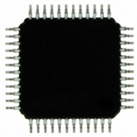
C8051F501-IQ Silicon Laboratories Inc, C8051F501-IQ Datasheet - Page 22

C8051F501-IQ
Manufacturer Part Number
C8051F501-IQ
Description
IC 8051 MCU 64K FLASH 48-QFP
Manufacturer
Silicon Laboratories Inc
Series
C8051F50xr
Specifications of C8051F501-IQ
Program Memory Type
FLASH
Program Memory Size
64KB (64K x 8)
Package / Case
48-QFP
Mfg Application Notes
LIN Bootloader AppNote
Core Processor
8051
Core Size
8-Bit
Speed
50MHz
Connectivity
EBI/EMI, SMBus (2-Wire/I²C), SPI, UART/USART
Peripherals
POR, PWM, Temp Sensor, WDT
Number Of I /o
40
Ram Size
4.25K x 8
Voltage - Supply (vcc/vdd)
1.8 V ~ 5.25 V
Data Converters
A/D 32x12b
Oscillator Type
Internal
Operating Temperature
-40°C ~ 125°C
Processor Series
C8051F5x
Core
8051
Data Bus Width
8 bit
Data Ram Size
4.25 KB
Interface Type
I2C/SPI/UART
Maximum Clock Frequency
50 MHz
Number Of Programmable I/os
40
Number Of Timers
4
Maximum Operating Temperature
+ 125 C
Mounting Style
SMD/SMT
3rd Party Development Tools
PK51, CA51, A51, ULINK2
Development Tools By Supplier
C8051F500DK
Minimum Operating Temperature
- 40 C
On-chip Adc
32-ch x 12-bit
Package
48PQFP
Device Core
8051
Family Name
C8051F50x
Maximum Speed
50 MHz
Operating Supply Voltage
2.5|3.3|5 V
Lead Free Status / RoHS Status
Lead free / RoHS Compliant
For Use With
336-1527 - KIT DEV FOR C8051F50X
Eeprom Size
-
Lead Free Status / Rohs Status
Lead free / RoHS Compliant
Other names
336-1512
Available stocks
Company
Part Number
Manufacturer
Quantity
Price
Company:
Part Number:
C8051F501-IQ
Manufacturer:
Silicon Laboratories Inc
Quantity:
10 000
Company:
Part Number:
C8051F501-IQR
Manufacturer:
Silicon Laboratories Inc
Quantity:
10 000
- Current page: 22 of 312
- Download datasheet (3Mb)
C8051F50x/F51x
3. Pin Definitions
22
VDD
GND
VDDA
GNDA
VREGIN
VIO
RST/
C2CK
C2D
P4.0/
C2D
P3.0/
C2D
P0.0
P0.1
P0.2
P0.3
P0.4
P0.5
Name
‘F500/1/4/5
(48-pin)
Pin
12
48
47
46
45
11
—
—
4
6
5
7
3
2
8
1
Table 3.1. Pin Definitions for the C8051F50x/F51x
(40-pin)
F508/9-
F510/1
Pin
10
—
40
39
38
37
4
6
5
7
3
2
9
8
1
‘F502/3/6/7
(32-pin)
Pin
10
32
31
30
29
—
—
4
6
5
7
3
2
9
8
1
D I/O
D I/O
D I/O
D I/O or A In
D I/O
D I/O or A In
D I/O
D I/O or A In Port 0.0. See SFR Definition 20.12 for a
D I/O or A In Port 0.1
D I/O or A In Port 0.2
D I/O or A In Port 0.3
D I/O or A In Port 0.4
D I/O or A In Port 0.5
Rev. 1.2
Type
Digital Supply Voltage. Must be connected.
Digital Ground. Must be connected.
Analog Supply Voltage. Must be connected.
Analog Ground. Must be connected.
Voltage Regulator Input
Port I/O Supply Voltage. Must be connected.
Device Reset. Open-drain output of internal
POR or V
can initiate a system reset by driving this pin
low.
Clock signal for the C2 Debug Interface.
Bi-directional data signal for the C2 Debug
Interface.
Port 4.0. See SFR Definition 20.29 for a
description.
Bi-directional data signal for the C2 Debug
Interface.
Port 3.0. See SFR Definition 20.24 for a
description.
Bi-directional data signal for the C2 Debug
Interface.
description.
DD
Monitor. An external source
Description
Related parts for C8051F501-IQ
Image
Part Number
Description
Manufacturer
Datasheet
Request
R
Part Number:
Description:
SMD/C°/SINGLE-ENDED OUTPUT SILICON OSCILLATOR
Manufacturer:
Silicon Laboratories Inc
Part Number:
Description:
Manufacturer:
Silicon Laboratories Inc
Datasheet:
Part Number:
Description:
N/A N/A/SI4010 AES KEYFOB DEMO WITH LCD RX
Manufacturer:
Silicon Laboratories Inc
Datasheet:
Part Number:
Description:
N/A N/A/SI4010 SIMPLIFIED KEY FOB DEMO WITH LED RX
Manufacturer:
Silicon Laboratories Inc
Datasheet:
Part Number:
Description:
N/A/-40 TO 85 OC/EZLINK MODULE; F930/4432 HIGH BAND (REV E/B1)
Manufacturer:
Silicon Laboratories Inc
Part Number:
Description:
EZLink Module; F930/4432 Low Band (rev e/B1)
Manufacturer:
Silicon Laboratories Inc
Part Number:
Description:
I°/4460 10 DBM RADIO TEST CARD 434 MHZ
Manufacturer:
Silicon Laboratories Inc
Part Number:
Description:
I°/4461 14 DBM RADIO TEST CARD 868 MHZ
Manufacturer:
Silicon Laboratories Inc
Part Number:
Description:
I°/4463 20 DBM RFSWITCH RADIO TEST CARD 460 MHZ
Manufacturer:
Silicon Laboratories Inc
Part Number:
Description:
I°/4463 20 DBM RADIO TEST CARD 868 MHZ
Manufacturer:
Silicon Laboratories Inc
Part Number:
Description:
I°/4463 27 DBM RADIO TEST CARD 868 MHZ
Manufacturer:
Silicon Laboratories Inc
Part Number:
Description:
I°/4463 SKYWORKS 30 DBM RADIO TEST CARD 915 MHZ
Manufacturer:
Silicon Laboratories Inc
Part Number:
Description:
N/A N/A/-40 TO 85 OC/4463 RFMD 30 DBM RADIO TEST CARD 915 MHZ
Manufacturer:
Silicon Laboratories Inc
Part Number:
Description:
I°/4463 20 DBM RADIO TEST CARD 169 MHZ
Manufacturer:
Silicon Laboratories Inc


