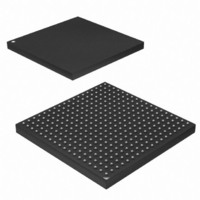
AT91SAM9G45-CU Atmel, AT91SAM9G45-CU Datasheet - Page 947

AT91SAM9G45-CU
Manufacturer Part Number
AT91SAM9G45-CU
Description
MCU ARM9 324-TFBGA
Manufacturer
Atmel
Series
AT91SAMr
Datasheets
1.AT91SAM9G45-EKES.pdf
(56 pages)
2.AT91SAM9G45-EKES.pdf
(1218 pages)
3.AT91SAM9G45-CU.pdf
(10 pages)
Specifications of AT91SAM9G45-CU
Core Processor
ARM9
Core Size
16/32-Bit
Speed
400MHz
Connectivity
EBI/EMI, Ethernet, I²C, IrDA, MMC, SPI, SSC, UART/USART, USB
Peripherals
AC'97, DMA, I²S, LCD, POR, PWM, WDT
Number Of I /o
160
Program Memory Size
64KB (64K x 8)
Program Memory Type
ROM
Ram Size
128K x 8
Voltage - Supply (vcc/vdd)
0.9 V ~ 1.1 V
Data Converters
A/D 8x10b
Oscillator Type
Internal
Operating Temperature
-40°C ~ 85°C
Package / Case
324-TFBGA
Processor Series
AT91SAMx
Core
ARM926EJ-S
Data Bus Width
32 bit
Data Ram Size
64 KB
Interface Type
I2C, SPI, UART
Maximum Clock Frequency
800 MHz
Number Of Programmable I/os
160
Number Of Timers
5
Maximum Operating Temperature
+ 85 C
Mounting Style
SMD/SMT
3rd Party Development Tools
JTRACE-ARM-2M, MDK-ARM, RL-ARM, ULINK2
Development Tools By Supplier
AT91SAM-ICE, AT91-ISP
Minimum Operating Temperature
- 40 C
On-chip Adc
10 bit
Controller Family/series
AT91
No. Of I/o's
160
Ram Memory Size
64KB
Cpu Speed
400MHz
No. Of Timers
2
Rohs Compliant
Yes
For Use With
AT91SAM9G45-EKES - KIT EVAL FOR AT91SAM9G45
Lead Free Status / RoHS Status
Lead free / RoHS Compliant
Eeprom Size
-
Lead Free Status / Rohs Status
Lead free / RoHS Compliant
Available stocks
Company
Part Number
Manufacturer
Quantity
Price
Company:
Part Number:
AT91SAM9G45-CU
Manufacturer:
ATMEL
Quantity:
1 000
Company:
Part Number:
AT91SAM9G45-CU
Manufacturer:
Atmel
Quantity:
31
Part Number:
AT91SAM9G45-CU
Manufacturer:
ATMEL/爱特梅尔
Quantity:
20 000
- Current page: 947 of 1218
- Download datasheet (19Mb)
40.10.2
6438F–ATARM–21-Jun-10
Touch Screen Mode
If the PDC is enabled, all the converted data are transferred contiguously in the memory buffer.
The bit LOWRES defines which resolution is used, either 8-bit or 10-bit, and thus the width of the
PDC memory buffer.
Writing TSAMOD to “Touch Screen Only Mode” automatically enables the touch screen pins as
analog inputs, and thus disables the digital function of the corresponding pins.
In Touch Screen Mode, the channels 0 to 3 corresponding to the Touch Screen inputs are auto-
matically activated and the bits CH0 to CH3 are automatically set in the
Status
The remaining channels can be either enabled or disabled by the user and their conversions are
performed at the end of each touch screen sequence.
The resolution is forced to 10 bits, regardless of the LOWRES bit setting.
At each trigger, if the bit PRES in
is performed to measure only position.
The resulting buffer is 16 bits wide and its structure stored in memory is:
5. If Channel 1 is enabled, convert Channel 1 and store result in both TSADCC_CDR1
6. If Channel 2 is enabled, convert Channel 2 and store result in both TSADCC_CDR2
7. If Channel 3 is enabled, convert Channel 3 and store result in both TSADCC_CDR3
8. If Channel 4 to Channel 7 are enabled, convert the Channels and store result in the cor-
9. If SLEEP is set, sleep down the ADC cell.
1. If SLEEP is set, wake up the ADC cell and wait for the Startup Time.
2. Close the switches on the inputs X
3. Convert Channel X
4. Close the switches on the inputs X
5. Convert Channel X
6. Close the switches on the inputs X
7. Convert Channel Y
8. Close the switches on the inputs Y
9. Convert Channel Y
10. Close the switches on the inputs Y
11. Convert Channel Y
12. Close the switches on the inputs Y
13. Convert Channel X
14. If Channel 4 to Channel 7 are enabled, convert the Channels and store result in the cor-
15. If SLEEP is set, sleep down the ADC cell.
and TSADCC_LCDR.
and TSADCC_LCDR.
and TSADCC_LCDR.
responding TSADCC_CDRx and TSADCC_LCDR.
result in both TSADCC_CDR0 and TSADCC_LCDR.
result in both TSADCC_CDR1 and TSADCC_LCDR.
result in both TSADCC_CDR2 and TSADCC_LCDR.
result in both TSADCC_CDR3 and TSADCC_LCDR.
responding TSADCC_CDRx and TSADCC_LCDR.
Register”.
P
P
P
P
M
M
, subtract TSADCC_CDR1 from the result and store the subtraction
, subtract TSADCC_CDR1 from the result and store the subtraction
, subtract TSADCC_CDR3 from the result and store the subtraction
, subtract TSADCC_CDR3 from the result and store the subtraction
and store the result in TSADCC_CDR1.
and store the result in TSADCC_CDR3.
“TSADCC Mode Register”
P
P
P
P
P
P
and X
and X
and X
and Y
and Y
and Y
M
M
M
M
M
M
during the Sample and Hold Time.
during the Sample and Hold Time.
during the Sample and Hold Time.
during the Sample and Hold Time.
during the Sample and Hold Time.
during the Sample and Hold Time.
is disabled, the following sequence
AT91SAM9G45
“TSADCC Channel
947
Related parts for AT91SAM9G45-CU
Image
Part Number
Description
Manufacturer
Datasheet
Request
R

Part Number:
Description:
MCU, MPU & DSP Development Tools KICKSTART KIT FOR AT91SAM9 PLUS
Manufacturer:
IAR Systems

Part Number:
Description:
DEV KIT FOR AVR/AVR32
Manufacturer:
Atmel
Datasheet:

Part Number:
Description:
INTERVAL AND WIPE/WASH WIPER CONTROL IC WITH DELAY
Manufacturer:
ATMEL Corporation
Datasheet:

Part Number:
Description:
Low-Voltage Voice-Switched IC for Hands-Free Operation
Manufacturer:
ATMEL Corporation
Datasheet:

Part Number:
Description:
MONOLITHIC INTEGRATED FEATUREPHONE CIRCUIT
Manufacturer:
ATMEL Corporation
Datasheet:

Part Number:
Description:
AM-FM Receiver IC U4255BM-M
Manufacturer:
ATMEL Corporation
Datasheet:

Part Number:
Description:
Monolithic Integrated Feature Phone Circuit
Manufacturer:
ATMEL Corporation
Datasheet:

Part Number:
Description:
Multistandard Video-IF and Quasi Parallel Sound Processing
Manufacturer:
ATMEL Corporation
Datasheet:

Part Number:
Description:
High-performance EE PLD
Manufacturer:
ATMEL Corporation
Datasheet:

Part Number:
Description:
8-bit Flash Microcontroller
Manufacturer:
ATMEL Corporation
Datasheet:

Part Number:
Description:
2-Wire Serial EEPROM
Manufacturer:
ATMEL Corporation
Datasheet:


