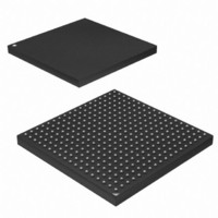
AT91SAM9G45-CU Atmel, AT91SAM9G45-CU Datasheet - Page 1189

AT91SAM9G45-CU
Manufacturer Part Number
AT91SAM9G45-CU
Description
MCU ARM9 324-TFBGA
Manufacturer
Atmel
Series
AT91SAMr
Datasheets
1.AT91SAM9G45-EKES.pdf
(56 pages)
2.AT91SAM9G45-EKES.pdf
(1218 pages)
3.AT91SAM9G45-CU.pdf
(10 pages)
Specifications of AT91SAM9G45-CU
Core Processor
ARM9
Core Size
16/32-Bit
Speed
400MHz
Connectivity
EBI/EMI, Ethernet, I²C, IrDA, MMC, SPI, SSC, UART/USART, USB
Peripherals
AC'97, DMA, I²S, LCD, POR, PWM, WDT
Number Of I /o
160
Program Memory Size
64KB (64K x 8)
Program Memory Type
ROM
Ram Size
128K x 8
Voltage - Supply (vcc/vdd)
0.9 V ~ 1.1 V
Data Converters
A/D 8x10b
Oscillator Type
Internal
Operating Temperature
-40°C ~ 85°C
Package / Case
324-TFBGA
Processor Series
AT91SAMx
Core
ARM926EJ-S
Data Bus Width
32 bit
Data Ram Size
64 KB
Interface Type
I2C, SPI, UART
Maximum Clock Frequency
800 MHz
Number Of Programmable I/os
160
Number Of Timers
5
Maximum Operating Temperature
+ 85 C
Mounting Style
SMD/SMT
3rd Party Development Tools
JTRACE-ARM-2M, MDK-ARM, RL-ARM, ULINK2
Development Tools By Supplier
AT91SAM-ICE, AT91-ISP
Minimum Operating Temperature
- 40 C
On-chip Adc
10 bit
Controller Family/series
AT91
No. Of I/o's
160
Ram Memory Size
64KB
Cpu Speed
400MHz
No. Of Timers
2
Rohs Compliant
Yes
For Use With
AT91SAM9G45-EKES - KIT EVAL FOR AT91SAM9G45
Lead Free Status / RoHS Status
Lead free / RoHS Compliant
Eeprom Size
-
Lead Free Status / Rohs Status
Lead free / RoHS Compliant
Available stocks
Company
Part Number
Manufacturer
Quantity
Price
Company:
Part Number:
AT91SAM9G45-CU
Manufacturer:
ATMEL
Quantity:
1 000
Company:
Part Number:
AT91SAM9G45-CU
Manufacturer:
Atmel
Quantity:
31
Part Number:
AT91SAM9G45-CU
Manufacturer:
ATMEL/爱特梅尔
Quantity:
20 000
- Current page: 1189 of 1218
- Download datasheet (19Mb)
Figure 46-25. SPI Slave Mode - NPCS Timings
Table 46-46. UART SPI Timings with 3.3V Peripheral Supply
Notes:
6438F–ATARM–21-Jun-10
Symbol
SPI
SPI
SPI
SPI
SPI
SPI
SPI
SPI
SPI
SPI
SPI
SPI
SPI
SPI
SPI
SPI
SPI
0
1
2
3
4
5
6
7
8
9
10
11
12
13
14
15
16
1. For output signals, Min and Max access time must be extracted. The Min access time is the time between the SPCK rising or
falling edge and the signal change. The Max access time is the time between the SPCK rising or falling edge and the signal
stabilization.
Parameter
SPCK Period
Input Data Setup Time
Input Data Hold Time
Chip Select Active to Serial Clock
Output Data Setup Time
Serial Clock to Chip Select Inactive
SPCK falling to MISO
MOSI Setup time before SPCK rises
MOSI Hold time after SPCK rises
SPCK rising to MISO
MOSI Setup time before SPCK falls
MOSI Hold time after SPCK falls
NPCS0 setup to SPCK rising
NPCS0 hold after SPCK falling
NPCS0 setup to SPCK falling
NPCS0 hold after SPCK rising
NPCS0 falling to MISO valid
Figure 46-9
(CPOL = 0)
(CPOL = 1)
MISO
SPCK
SPCK
illustrates Min and Max accesses for SPI2. The same applies to SPI5, SPI6, SPI9.
SPI
SPI
SPI
16
12
14
SPI
6
SPI
9
Master Mode
Slave Mode
Cond
13.8
4.7
17.2
10.3
10.7
Min
7.5
0.4
2.0
2.0
2.9
0
0
(1)
(1)
SPI
SPI
15
13
AT91SAM9G45
16.9
17.1
Max
16.0
-0.3
3.5
0.2
(1)
(1)
Units
ns
ns
ns
ns
ns
ns
ns
ns
ns
ns
ns
ns
ns
ns
ns
ns
ns
1189
Related parts for AT91SAM9G45-CU
Image
Part Number
Description
Manufacturer
Datasheet
Request
R

Part Number:
Description:
MCU, MPU & DSP Development Tools KICKSTART KIT FOR AT91SAM9 PLUS
Manufacturer:
IAR Systems

Part Number:
Description:
DEV KIT FOR AVR/AVR32
Manufacturer:
Atmel
Datasheet:

Part Number:
Description:
INTERVAL AND WIPE/WASH WIPER CONTROL IC WITH DELAY
Manufacturer:
ATMEL Corporation
Datasheet:

Part Number:
Description:
Low-Voltage Voice-Switched IC for Hands-Free Operation
Manufacturer:
ATMEL Corporation
Datasheet:

Part Number:
Description:
MONOLITHIC INTEGRATED FEATUREPHONE CIRCUIT
Manufacturer:
ATMEL Corporation
Datasheet:

Part Number:
Description:
AM-FM Receiver IC U4255BM-M
Manufacturer:
ATMEL Corporation
Datasheet:

Part Number:
Description:
Monolithic Integrated Feature Phone Circuit
Manufacturer:
ATMEL Corporation
Datasheet:

Part Number:
Description:
Multistandard Video-IF and Quasi Parallel Sound Processing
Manufacturer:
ATMEL Corporation
Datasheet:

Part Number:
Description:
High-performance EE PLD
Manufacturer:
ATMEL Corporation
Datasheet:

Part Number:
Description:
8-bit Flash Microcontroller
Manufacturer:
ATMEL Corporation
Datasheet:

Part Number:
Description:
2-Wire Serial EEPROM
Manufacturer:
ATMEL Corporation
Datasheet:


