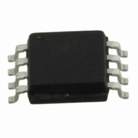
W25Q80BVSSIG Winbond Electronics, W25Q80BVSSIG Datasheet - Page 40

W25Q80BVSSIG
Manufacturer Part Number
W25Q80BVSSIG
Description
IC FLASH 8MBIT 8SOIC
Manufacturer
Winbond Electronics
Datasheet
1.W25Q80BVSSIG.pdf
(75 pages)
Specifications of W25Q80BVSSIG
Format - Memory
FLASH
Memory Type
FLASH
Memory Size
8M (1M x 8)
Speed
104MHz
Interface
SPI Serial
Voltage - Supply
2.7 V ~ 3.6 V
Operating Temperature
-40°C ~ 85°C
Package / Case
8-SOIC (5.3mm Width), 8-SOP, 8-SOEIAJ
Lead Free Status / RoHS Status
Lead free / RoHS Compliant
Other names
Q4816329
T1015683
T1015683
Available stocks
Company
Part Number
Manufacturer
Quantity
Price
Company:
Part Number:
W25Q80BVSSIG
Manufacturer:
Winbond
Quantity:
2 100
Company:
Part Number:
W25Q80BVSSIG
Manufacturer:
WINBOND
Quantity:
192
Part Number:
W25Q80BVSSIG
Manufacturer:
WINBOND/华邦
Quantity:
20 000
9.2.22
The Quad Page Program instruction allows up to 256 bytes of data to be programmed at previously
erased (FFh) memory locations using four pins: IO
improve performance for PROM Programmer and applications that have slow clock speeds <5MHz.
Systems with faster clock speed will not realize much benefit for the Quad Page Program instruction
since the inherent page program time is much greater than the time it take to clock-in the data.
To use Quad Page Program the Quad Enable in Status Register-2 must be set (QE=1). A Write Enable
instruction must be executed before the device will accept the Quad Page Program instruction (Status
Register-1, WEL=1). The instruction is initiated by driving the /CS pin low then shifting the instruction
code “32h” followed by a 24-bit address (A23-A0) and at least one data byte, into the IO pins. The /CS pin
must be held low for the entire length of the instruction while data is being sent to the device. All other
functions of Quad Page Program are identical to standard Page Program. The Quad Page Program
instruction sequence is shown in figure 20.
Quad Input Page Program (32h)
CLK
CLK
/CS
/CS
IO
IO
IO
IO
IO
IO
IO
IO
0
1
2
3
0
1
2
3
Mode 3
Mode 0
0
31
*
= MSB
Byte 1
*
4
5
6
7
32
0
1
2
3
Figure 20. Quad Input Page Program Instruction Sequence Diagram
33
0
*
Byte 2
4
5
6
7
34
1
0
1
2
3
35
Instruction (32h)
2
Byte 3
*
4
5
6
7
36
3
0
1
2
3
37
4
5
- 40 -
6
0
, IO
*
4
5
6
7
Byte
253
7
1
0
1
2
3
, IO
23
*
8
*
4
5
6
7
2
22
Byte
254
, and IO
9
0
1
2
3
21
10
24-Bit Address
*
4
5
6
7
Byte
255
3
. The Quad Page Program can
0
1
2
3
3
28
*
4
5
6
7
Byte
2
256
29
0
1
2
3
1
30
W25Q80BV
0
31
Mode 3
Mode 0


