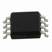
W25Q80BVSSIG Winbond Electronics, W25Q80BVSSIG Datasheet - Page 24

W25Q80BVSSIG
Manufacturer Part Number
W25Q80BVSSIG
Description
IC FLASH 8MBIT 8SOIC
Manufacturer
Winbond Electronics
Datasheet
1.W25Q80BVSSIG.pdf
(75 pages)
Specifications of W25Q80BVSSIG
Format - Memory
FLASH
Memory Type
FLASH
Memory Size
8M (1M x 8)
Speed
104MHz
Interface
SPI Serial
Voltage - Supply
2.7 V ~ 3.6 V
Operating Temperature
-40°C ~ 85°C
Package / Case
8-SOIC (5.3mm Width), 8-SOP, 8-SOEIAJ
Lead Free Status / RoHS Status
Lead free / RoHS Compliant
Other names
Q4816329
T1015683
T1015683
Available stocks
Company
Part Number
Manufacturer
Quantity
Price
Company:
Part Number:
W25Q80BVSSIG
Manufacturer:
Winbond
Quantity:
2 100
Company:
Part Number:
W25Q80BVSSIG
Manufacturer:
WINBOND
Quantity:
192
Part Number:
W25Q80BVSSIG
Manufacturer:
WINBOND/华邦
Quantity:
20 000
To complete the Write Status Register instruction, the /CS pin must be driven high after the eighth or
sixteenth bit of data that is clocked in. If this is not done the Write Status Register instruction will not be
executed. If /CS is driven high after the eighth clock (compatible with the 25X series) the CMP and QE
bits will be cleared to 0.
During non-volatile Status Register write operation (06h combined with 01h), after /CS is driven high, the
self-timed Write Status Register cycle will commence for a time duration of t
While the Write Status Register cycle is in progress, the Read Status Register instruction may still be
accessed to check the status of the BUSY bit. The BUSY bit is a 1 during the Write Status Register cycle
and a 0 when the cycle is finished and ready to accept other instructions again. After the Write Status
Register cycle has finished, the Write Enable Latch (WEL) bit in the Status Register will be cleared to 0.
During volatile Status Register write operation (50h combined with 01h), after /CS is driven high, the
Status Register bits will be refreshed to the new values within the time period of t
Characteristics). BUSY bit will remain 0 during the Status Register bit refresh period.
Please refer to 9.1 for detailed Status Register Bit descriptions. Factory default for all status Register bits
are 0.
(IO
(IO
CLK
/CS
DO
DI
0
1
)
)
Mode 3
Mode 0
*
= MSB
0
1
Instruction (01h)
2
3
Figure 8. Write Status Register Instruction Sequence Diagram
4
5
6
7
*
7
8
6
9
Status Register 1 in
High Impedance
5
10
- 24 -
4
11
3
12
2
13
1
14
0
15
15
*
16
14
17
Status Register 2 in
13
18
W
12
(See AC Characteristics).
19
11
20
W25Q80BV
10
21
SHSL2
9
22
8
23
(See AC
Mode 3
Mode 0


