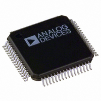
ADV7343BSTZ Analog Devices Inc, ADV7343BSTZ Datasheet - Page 68

ADV7343BSTZ
Manufacturer Part Number
ADV7343BSTZ
Description
IC ENCODER VIDEO W/DAC 64-LQFP
Manufacturer
Analog Devices Inc
Type
Video Encoderr
Datasheet
1.ADV7343BSTZ.pdf
(104 pages)
Specifications of ADV7343BSTZ
Applications
DVD, Blu-Ray
Voltage - Supply, Analog
3.3V
Voltage - Supply, Digital
1.8V
Mounting Type
Surface Mount
Package / Case
64-LQFP
Supply Voltage Range
1.71V To 1.89V
Operating Temperature Range
-40°C To +85°C
Tv / Video Case Style
LQFP
No. Of Pins
64
Svhc
No SVHC (18-Jun-2010)
Operating Temperature Max
85°C
Operating
RoHS Compliant
Input Format
Digital
Output Format
Analogue
Dac Resolution
11bit
Rohs Compliant
Yes
Lead Free Status / RoHS Status
Lead free / RoHS Compliant
Available stocks
Company
Part Number
Manufacturer
Quantity
Price
Company:
Part Number:
ADV7343BSTZ
Manufacturer:
ADI
Quantity:
301
Company:
Part Number:
ADV7343BSTZ
Manufacturer:
Analog Devices Inc
Quantity:
10 000
Part Number:
ADV7343BSTZ
Manufacturer:
ADI/亚德诺
Quantity:
20 000
Company:
Part Number:
ADV7343BSTZ-3
Manufacturer:
ADI
Quantity:
246
ADV7342/ADV7343
SLEEP MODE
Subaddress 0x00, Bit 0
In sleep mode, most of the digital I/O pins of the ADV7340/
ADV7341 are disabled. For inputs, this means that the external
data is ignored, and internally the logic normally driven by a
given input is just tied low or high. This includes CLKINx.
For digital output pins, this means that the pin goes into tristate
(high impedance) mode.
There are some exceptions to allow the user to continue to
communicate with the part via I
pins are kept alive.
PIXEL AND CONTROL PORT READBACK
Subaddress 0x12 to Subaddress 0x14, Subaddress 0x16
The ADV7342/ADV7343 support the readback of most digital
inputs via the I
level connectivity testing with upstream devices.
The pixel port (S[7:0], Y[7:0], and C[7:0]), the control port
( S_HSYNC , S_VSYNC , P_HSYNC , P_VSYNC , and P_BLANK ),
and the SFL pin are available for readback via the MPU port.
The readback registers are located at Subaddress 0x12 to
Subaddress 0x14 and Subaddress 0x16.
When using this feature, apply a clock signal to the CLKIN_A
pin to register the levels applied to the input pins.
RESET MECHANISM
Subaddress 0x17, Bit 1
The ADV7342/ADV7343 have a software reset accessible via
the I
a 1 to Subaddress 0x17, Bit 1. This resets all registers to their
default values. This bit is self-clearing; that is, after a 1 has been
written to the bit, the bit automatically returns to 0.
2
C MPU port. A software reset is activated by writing
2
C MPU port. This feature is useful for board
TELETEXT VBI LINE
2
C: the ALSB, SDA, and SCL
Figure 84. Teletext VBI Line
Rev. A | Page 68 of 104
RUN-IN CLOCK
45 BYTES (360 BITS) – PAL
ADDRESS AND DATA
The ADV7342/ADV7343 include a power-on reset (POR)
circuit to ensure correct operation after power-up.
SD TELETEXT INSERTION
Subaddress 0xC9 to Subaddress 0xCE
The ADV7342/ADV7343 support the insertion of teletext data,
using a 2-pin interface, when operating in PAL mode. Teletext
insertion is enabled using Subaddress 0xC9, Bit 0.
In accordance with the PAL WST teletext standard, teletext data
should be inserted into the ADV7342/ADV7343 at a rate of
6.9375 Mbps. The teletext data can be inserted on the
S_VSYNC , P_VSYNC , or C0 pin. The pin on which the teletext
data is inserted is selected using Subaddress 0xC9, Bits [3:2].
When teletext insertion is enabled, a teletext request signal is
output from the ADV7342/ADV7343 to indicate when teletext
data should be inserted. The teletext request signal is output on
the SFL pin. The position (relative to the teletext data) and
width of the request signal are configurable using Subaddress
0xCA. The request signal can operate in either a line or a bit
mode. The request signal mode is controlled using Subaddress
0xC9, Bit 1.
To account for the noninteger relationship between the teletext
insertion rate (6.9375 Mbps) and the pixel clock (27 MHz), a
teletext insertion protocol is implemented in the ADV7342/
ADV7343. At a rate of 6.9375 Mbps, the time taken for the
insertion of 37 teletext bits equates to 144 pixel clock cycles (at
27 MHz). For every 37 teletext bits inserted into the ADV7342/
ADV7343, the 10
pixel clock cycles, and the remainder are carried for four pixel
clock cycles (totaling 144 pixel clock cycles). The teletext
insertion protocol repeats every 37 teletext bits or 144 pixel
clock cycles until all 360 teletext bits are inserted.
th
, 19
th
, 28
th,
and 37
th
bits are carried for three


