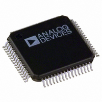
ADV7343BSTZ Analog Devices Inc, ADV7343BSTZ Datasheet - Page 27

ADV7343BSTZ
Manufacturer Part Number
ADV7343BSTZ
Description
IC ENCODER VIDEO W/DAC 64-LQFP
Manufacturer
Analog Devices Inc
Type
Video Encoderr
Datasheet
1.ADV7343BSTZ.pdf
(104 pages)
Specifications of ADV7343BSTZ
Applications
DVD, Blu-Ray
Voltage - Supply, Analog
3.3V
Voltage - Supply, Digital
1.8V
Mounting Type
Surface Mount
Package / Case
64-LQFP
Supply Voltage Range
1.71V To 1.89V
Operating Temperature Range
-40°C To +85°C
Tv / Video Case Style
LQFP
No. Of Pins
64
Svhc
No SVHC (18-Jun-2010)
Operating Temperature Max
85°C
Operating
RoHS Compliant
Input Format
Digital
Output Format
Analogue
Dac Resolution
11bit
Rohs Compliant
Yes
Lead Free Status / RoHS Status
Lead free / RoHS Compliant
Available stocks
Company
Part Number
Manufacturer
Quantity
Price
Company:
Part Number:
ADV7343BSTZ
Manufacturer:
ADI
Quantity:
301
Company:
Part Number:
ADV7343BSTZ
Manufacturer:
Analog Devices Inc
Quantity:
10 000
Part Number:
ADV7343BSTZ
Manufacturer:
ADI/亚德诺
Quantity:
20 000
Company:
Part Number:
ADV7343BSTZ-3
Manufacturer:
ADI
Quantity:
246
MPU PORT DESCRIPTION
Devices such as a microprocessor can communicate with the
ADV7342/ADV7343 through a 2-wire serial (I
bus. After power-up or reset, the MPU port is configured for
I
with the register map via SPI, contact Analog Devices, Inc.
I
The ADV7342/ADV7343 support a 2-wire serial (I
microprocessor bus driving multiple peripherals. This port
operates in an open-drain configuration. Two wires, serial data
(SDA) and serial clock (SCL), carry information between any
device connected to the bus and the ADV7342/ADV7343. The
slave address of the device depends on the device (ADV7342 or
ADV7343), the operation (read or write), and the state of the
ALSB pin (0 or 1). See Table 16, Figure 47, and Figure 48. The LSB
sets either a read or a write operation. Logic 1 corresponds to a
read operation, and Logic 0 corresponds to a write operation.
A1 is controlled by setting the ALSB pin of the ADV7342/
ADV7343 to Logic 0 or Logic 1.
Table 16. ADV7342/ADV7343 I
Device
ADV7342
ADV7343
Analog Devices, Inc., recommends tying up ALSB. If this is not
done, a power supply sequence (PSS) may be required. For more
information on the PSS, see the Power Supply Sequencing section.
2
2
C operation. To obtain information about communicating
C OPERATION
0
1
ALSB
0
0
1
1
0
0
1
1
1
1
Figure 47. ADV7342 I
Figure 48. ADV7343 I
0
0
1
1
0
0
Operation
Write
Read
Write
Read
Write
Read
Write
Read
2
2
2
C Slave Addresses
C Slave Address
C Slave Address
1
SET UP BY
1
ADDRESS
CONTROL
CONTROL
SET UP BY
ADDRESS
ALSB
ALSB
A1
A1
READ/WRITE
READ/WRITE
CONTROL
0
1
CONTROL
0
1
2
WRITE
READ
WRITE
READ
X
C-compatible)
X
Slave Address
0xD4
0xD5
0xD6
0xD7
0x54
0x55
0x56
0x57
2
C-compatible)
Rev. A | Page 27 of 104
The various devices on the bus use the following protocol. The
master initiates a data transfer by establishing a start condition,
defined by a high-to-low transition on SDA while SCL remains
high. This indicates that an address/data stream follows. All
peripherals respond to the start condition and shift the next
eight bits (7-bit address plus the R/ W bit). The bits are
transferred from MSB down to LSB. The peripheral that
recognizes the transmitted address responds by pulling the data
line low during the ninth clock pulse. This is known as an
acknowledge bit. All other devices withdraw from the bus at
this point and maintain an idle condition. The idle condition
occurs when the device monitors the SDA and SCL lines
waiting for the start condition and the correct transmitted
address. The R/ W bit determines the direction of the data.
Logic 0 on the LSB of the first byte means that the master writes
information to the peripheral. Logic 1 on the LSB of the first byte
means that the master reads information from the peripheral.
The ADV7342/ADV7343 act as a standard slave device on the
bus. The data on the SDA pin is eight bits long, supporting the
7-bit addresses plus the R/ W bit. It interprets the first byte as
the device address and the second byte as the starting subaddress.
There is a subaddress auto-increment facility. This allows data
to be written to or read from registers in ascending subaddress
sequence starting at any valid subaddress. A data transfer is
always terminated by a stop condition. The user can also access
any unique subaddress register on a one-by-one basis without
updating all the registers.
Stop and start conditions can be detected at any stage during the
data transfer. If these conditions are asserted out of sequence with
normal read and write operations, they cause an immediate jump
to the idle condition. During a given SCL high period, the user
should issue only a start condition, a stop condition, or a stop
condition followed by a start condition. If an invalid subaddress
is issued by the user, the ADV7342/ADV7343 do not issue an
acknowledge but return to the idle condition. If the user uses the
auto-increment method of addressing the encoder and exceeds
the highest subaddress, the following actions are taken:
•
•
Figure 49 shows data transfer for a write sequence and the start
and stop conditions. Figure 50 shows bus write and read sequences.
In read mode, the highest subaddress register contents are
output until the master device issues a no acknowledge.
This indicates the end of a read. A no acknowledge condition
occurs when the SDA line is not pulled low on the ninth pulse.
In write mode, the data for the invalid byte is not loaded
into any subaddress register, a no acknowledge is issued by
the ADV7342/ADV7343, and the parts return to the idle
condition.
ADV7342/ADV7343


