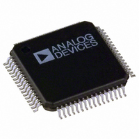
ADV7343BSTZ Analog Devices Inc, ADV7343BSTZ Datasheet - Page 29

ADV7343BSTZ
Manufacturer Part Number
ADV7343BSTZ
Description
IC ENCODER VIDEO W/DAC 64-LQFP
Manufacturer
Analog Devices Inc
Type
Video Encoderr
Datasheet
1.ADV7343BSTZ.pdf
(104 pages)
Specifications of ADV7343BSTZ
Applications
DVD, Blu-Ray
Voltage - Supply, Analog
3.3V
Voltage - Supply, Digital
1.8V
Mounting Type
Surface Mount
Package / Case
64-LQFP
Supply Voltage Range
1.71V To 1.89V
Operating Temperature Range
-40°C To +85°C
Tv / Video Case Style
LQFP
No. Of Pins
64
Svhc
No SVHC (18-Jun-2010)
Operating Temperature Max
85°C
Operating
RoHS Compliant
Input Format
Digital
Output Format
Analogue
Dac Resolution
11bit
Rohs Compliant
Yes
Lead Free Status / RoHS Status
Lead free / RoHS Compliant
Available stocks
Company
Part Number
Manufacturer
Quantity
Price
Company:
Part Number:
ADV7343BSTZ
Manufacturer:
ADI
Quantity:
301
Company:
Part Number:
ADV7343BSTZ
Manufacturer:
Analog Devices Inc
Quantity:
10 000
Part Number:
ADV7343BSTZ
Manufacturer:
ADI/亚德诺
Quantity:
20 000
Company:
Part Number:
ADV7343BSTZ-3
Manufacturer:
ADI
Quantity:
246
REGISTER MAP ACCESS
A microprocessor can read from or write to all registers of the
ADV7342/ADV7343 via the MPU port, except for registers that
are specified as read-only or write-only registers.
The subaddress register determines which register the next
read or write operation accesses. All communication through
the MPU port starts with an access to the subaddress register.
A read/write operation is then performed from/to the target
address, which increments to the next address until the
transaction is complete.
Table 17. Register 0x00
SR7 to
SR0
0x00
Table 18. Register 0x01 to Register 0x09
SR7 to
SR0
0x01
Register
Power
mode
Mode select
Register
Bit Description
Sleep mode. With this control enabled, the current consumption is
reduced to μA level. All DACs and the internal PLL circuits are
disabled. Registers can be read from and written to in sleep mode.
PLL and oversampling control. This control allows the internal PLL 1
circuit to be powered down and the oversampling to be switched off.
DAC 3: power on/off.
DAC 2: power on/off.
DAC 1: power on/off.
DAC 6: power on/off.
DAC 5: power on/off.
DAC 4: power on/off.
Bit Description
Reserved.
DDR clock edge
alignment (only used
for ED-
modes)
Reserved.
Input mode (see
Register 0x30, Bits[7:3]
for ED/HD standard
selection)
Y/C/S bus swap
2
and HD-DDR
7
0
1
6
0
0
0
0
1
1
1
1
Rev. A | Page 29 of 104
5
0
0
1
1
0
0
1
1
Bit Number
4
0
1
0
1
0
1
0
1
3
0
REGISTER PROGRAMMING
Table 17 to Table 35 describe the functionality of each register.
All registers can be read from as well as written to, unless
otherwise stated.
SUBADDRESS REGISTER (SR7 TO SR0)
The subaddress register is an 8-bit write-only register. After the
MPU port is accessed and a read/write operation is selected, the
subaddress is set up. The subaddress register determines to or
from which register the operation takes place.
1
2
0
0
1
1
1
0
1
0
1
0
0
7
0
1
Register Setting
Chroma clocked in on rising clock edge;
luma clocked in on falling clock edge
Reserved
Reserved
Luma clocked in on rising clock edge;
chroma clocked in on falling clock edge
SD input only
ED/HD-SDR input only
ED/HD-DDR input only
SD and ED/HD-SDR
SD and ED/HD-DDR
Reserved
Reserved
ED only (at 54 MHz)
Allows data to be applied to data ports in
various configurations (SD feature only)
6
0
1
5
0
1
Bit Number
4
0
1
3
0
1
2
0
1
ADV7342/ADV7343
1
0
1
0
0
1
Register
Setting
Sleep
mode off
Sleep
mode on
PLL 1 on
PLL 1 off
DAC 3 off
DAC 3 on
DAC 2 off
DAC 2 on
DAC 1 off
DAC 1 on
DAC 6 off
DAC 6 on
DAC 5 off
DAC 5 on
DAC 4 off
DAC 4 on
Reset
Value
0x12
Reset
Value
0x00


