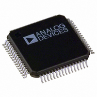
ADV7343BSTZ Analog Devices Inc, ADV7343BSTZ Datasheet - Page 21

ADV7343BSTZ
Manufacturer Part Number
ADV7343BSTZ
Description
IC ENCODER VIDEO W/DAC 64-LQFP
Manufacturer
Analog Devices Inc
Type
Video Encoderr
Datasheet
1.ADV7343BSTZ.pdf
(104 pages)
Specifications of ADV7343BSTZ
Applications
DVD, Blu-Ray
Voltage - Supply, Analog
3.3V
Voltage - Supply, Digital
1.8V
Mounting Type
Surface Mount
Package / Case
64-LQFP
Supply Voltage Range
1.71V To 1.89V
Operating Temperature Range
-40°C To +85°C
Tv / Video Case Style
LQFP
No. Of Pins
64
Svhc
No SVHC (18-Jun-2010)
Operating Temperature Max
85°C
Operating
RoHS Compliant
Input Format
Digital
Output Format
Analogue
Dac Resolution
11bit
Rohs Compliant
Yes
Lead Free Status / RoHS Status
Lead free / RoHS Compliant
Available stocks
Company
Part Number
Manufacturer
Quantity
Price
Company:
Part Number:
ADV7343BSTZ
Manufacturer:
ADI
Quantity:
301
Company:
Part Number:
ADV7343BSTZ
Manufacturer:
Analog Devices Inc
Quantity:
10 000
Part Number:
ADV7343BSTZ
Manufacturer:
ADI/亚德诺
Quantity:
20 000
Company:
Part Number:
ADV7343BSTZ-3
Manufacturer:
ADI
Quantity:
246
36
45, 35
44, 43, 42
39, 38, 37
21
20
19
46
41
10, 56
1
34
33
31
32
40
11, 57
64
1
2
ED = enhanced definition = 525p and 625p.
LSB = least significant bit. In the ADV7342, setting the LSB to 0 sets the I
LSB to 0 sets the I
R
COMP1,
COMP2
DAC 1, DAC 2,
DAC 3
DAC 4, DAC 5,
DAC 6
SCL
SDA
ALSB
V
V
V
V
PV
EXT_LF1
EXT_LF2
PGND
AGND
DGND
GND_IO
SET2
REF
AA
DD
DD_IO
2
DD
C address to 0x54. Setting it to 1 sets the I
I
O
O
O
I
I/O
I
P
P
P
P
I
I
G
G
G
G
External Loop Filter for On-Chip PLL 1.
External Loop Filter for On-Chip PLL 2.
Analog Ground Pin.
Digital Ground Pin.
This pin is used to control the amplitudes of the DAC 4, DAC 5, and DAC 6 outputs. A 4.12 kΩ
resistor must be connected from R
Compensation Pins. Connect a 2.2 nF capacitor from both COMP pins to V
DAC Outputs. Full- and low-drive capable DACs.
DAC Outputs. Low-drive only capable DACs.
I
I
This signal sets up the LSB
for more information).
Optional External Voltage Reference Input for DACs or Voltage Reference Output.
Analog Power Supply (3.3 V).
Digital Power Supply (1.8 V). For dual-supply configurations, V
supplies through a ferrite bead or suitable filtering.
Input/Output Digital Power Supply (1.8 V or 3.3 V).
PLL Power Supply (1.8 V). For dual-supply configurations, PV
supplies through a ferrite bead or suitable filtering.
PLL Ground Pin.
Input/Output Supply Ground Pin.
2
2
C Clock Input.
C Data Input/Output.
2
C address to 0x56.
2
Rev. A | Page 21 of 104
C address to 0xD4. Setting it to 1 sets the I
2
of the MPU I
SET2
to AGND.
2
C address (see the Power Supply Sequencing section
2
C address to 0xD6. In the ADV7343, setting the
DD
DD
can be connected to other 1.8 V
can be connected to other 1.8 V
ADV7342/ADV7343
AA
.


