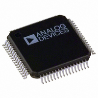
ADV7343BSTZ Analog Devices Inc, ADV7343BSTZ Datasheet - Page 47

ADV7343BSTZ
Manufacturer Part Number
ADV7343BSTZ
Description
IC ENCODER VIDEO W/DAC 64-LQFP
Manufacturer
Analog Devices Inc
Type
Video Encoderr
Datasheet
1.ADV7343BSTZ.pdf
(104 pages)
Specifications of ADV7343BSTZ
Applications
DVD, Blu-Ray
Voltage - Supply, Analog
3.3V
Voltage - Supply, Digital
1.8V
Mounting Type
Surface Mount
Package / Case
64-LQFP
Supply Voltage Range
1.71V To 1.89V
Operating Temperature Range
-40°C To +85°C
Tv / Video Case Style
LQFP
No. Of Pins
64
Svhc
No SVHC (18-Jun-2010)
Operating Temperature Max
85°C
Operating
RoHS Compliant
Input Format
Digital
Output Format
Analogue
Dac Resolution
11bit
Rohs Compliant
Yes
Lead Free Status / RoHS Status
Lead free / RoHS Compliant
Available stocks
Company
Part Number
Manufacturer
Quantity
Price
Company:
Part Number:
ADV7343BSTZ
Manufacturer:
ADI
Quantity:
301
Company:
Part Number:
ADV7343BSTZ
Manufacturer:
Analog Devices Inc
Quantity:
10 000
Part Number:
ADV7343BSTZ
Manufacturer:
ADI/亚德诺
Quantity:
20 000
Company:
Part Number:
ADV7343BSTZ-3
Manufacturer:
ADI
Quantity:
246
ADV7342/ADV7343
ENHANCED DEFINITION/HIGH DEFINITION ONLY
Subaddress 0x01, Bits[6:4] = 001 or 010
Enhanced definition (ED) or high definition (HD) YCrCb data
can be input in either 4:2:2 or 4:4:4 format. If desired, dual data
rate (DDR) pixel data inputs can be employed (4:2:2 format only).
Enhanced definition (ED) or high definition (HD) RGB data
can be input in 4:4:4 format (single data rate only).
The clock signal must be provided on the CLKIN_A pin. Input
synchronization signals are provided on the P_HSYNC , P_VSYNC ,
and P_BLANK pins.
16-Bit 4:2:2 YCrCb Mode (SDR)
Subaddress 0x35, Bit 1 = 0; Subaddress 0x33, Bit 6 = 1
In 16-bit 4:2:2 YCrCb input mode, the Y pixel data is input on
Pin Y7 to Pin Y0, with Pin Y0 being the LSB. The CrCb pixel
data is input on Pin C7 to Pin C0, with Pin C0 being the LSB.
8-Bit 4:2:2 YCrCb Mode (DDR)
Subaddress 0x35, Bit 1 = 0; Subaddress 0x33, Bit 6 = 1
In 8-bit DDR 4:2:2 YCrCb input mode, the Y pixel data is input
on Pin Y7 to Pin Y0 on either the rising or falling edge of
CLKIN_A. Pin Y0 is the LSB.
The CrCb pixel data is also input on Pin Y7 to Pin Y0 on the
opposite edge of CLKIN_A. Pin Y0 is the LSB. Whether the Y
data is clocked in on the rising or falling edge of CLKIN_A is
determined by Subaddress 0x01, Bits[2:1] (see Figure 52 and
Figure 53).
NOTES
1. SUBADDRESS 0x01 [2:1] SHOULD BE SET TO 00 IN THIS CASE.
CLKIN_ A
NOTES
1. SUBADDRESS 0x01 [2:1] SHOULD BE SET TO 11 IN THIS CASE.
CLKIN_A
Y[7:0]
Y[7:0]
Figure 52. ED/HD-DDR Input Sequence (EAV/SAV)—Option A
Figure 53. ED/HD-DDR Input Sequence (EAV/SAV)—Option B
*SELECTED BY SUBADDRESS 0x01, BIT 7.
3FF
3FF
DECODER
MPEG2
Figure 51. SD Only Example Application
YCrCb
00
00
00
00
27MHz
2
8
X Y
XY
CLKIN_A
S[7:0] OR Y[7:0]*
S_HSYNC
S_VSYNC,
Cb0
Y0
ADV7342/
ADV7343
Cb0
Y0
Cr0
Y1
Y1
Cr0
Rev. A | Page 47 of 104
24-Bit 4:4:4 YCrCb Mode
Subaddress 0x35, Bit 1 = 0; Subaddress 0x33, Bit 6 = 0
In 24-bit 4:4:4 YCrCb input mode, the Y pixel data is input on
Pin Y7 to Pin Y0, with Pin Y0 being the LSB.
The Cr pixel data is input on Pin S7 to Pin S0, with Pin S0 being
the LSB. The Cb pixel data is input on Pin C7 to Pin C0, with
Pin C0 being the LSB.
24-Bit 4:4:4 RGB Mode
Subaddress 0x35, Bit 1 = 1
In 24-bit 4:4:4 RGB input mode, the red pixel data is input on
Pin S7 to Pin S0, the green pixel data is input on Pin Y7 to Pin Y0,
and the blue pixel data is input on Pin C7 to Pin C0. The S0, Y0,
and C0 pins are the respective bus LSBs.
SIMULTANEOUS STANDARD DEFINITION AND
ENHANCED DEFINITION/HIGH DEFINITION
Subaddress 0x01, Bits[6:4] = 011 or 100
The ADV7342/ADV7343 are able to simultaneously process SD
4:2:2 YCrCb data and ED/HD 4:2:2 YCrCb data. The 27 MHz
SD clock signal must be provided on the CLKIN_A pin. The
ED/HD clock signal must be provided on the CLKIN_B pin.
SD input synchronization signals are provided on the S_HSYNC
and S_VSYNC pins. ED/HD input synchronization signals are
provided on the P_HSYNC , P_VSYNC and P_BLANK pins.
SD 8-Bit 4:2:2 YCrCb and ED/HD-SDR 16-Bit 4:2:2 YCrCb
The SD 8-bit 4:2:2 YCrCb pixel data is input on Pin S7 to Pin S0,
with Pin S0 being the LSB.
The ED/HD 16-bit 4:2:2 Y pixel data is input on Pin Y7 to Pin Y0,
with Pin Y0 being the LSB.
The ED/HD 16-bit 4:2:2 CrCb pixel data is input on Pin C7 to
Pin C0, with Pin C0 being the LSB.
SD 8-Bit 4:2:2 YCrCb and ED/HD-DDR 8-Bit 4:2:2 YCrCb
The SD 8-bit 4:2:2 YCrCb pixel data is input on Pin S7 to Pin S0,
with Pin S0 being the LSB. The ED/HD-DDR 8-bit 4:2:2 Y pixel
data is input on Pin Y7 to Pin Y0 on the rising or falling edge of
CLKIN_B. Pin Y0 is the LSB.
The ED/HD-DDR 8-bit 4:2:2 CrCb pixel data is also input on
Pin Y7 to Pin Y0 on the opposite edge of CLKIN_B. Pin Y0 is
the LSB.
INTERLACED TO
PROGRESSIVE
DECODER
MPEG2
YCrCb
Figure 54. ED/HD Only Example Application
Cb
Cr
Y
8
8
8
3
P_HSYNC,
P_BLANK
CLKIN_ A
C[7:0]
S[7:0]
Y[7:0]
P_VSYNC,
ADV7342/
ADV7343


