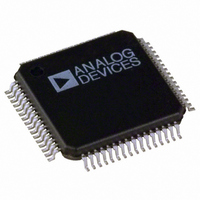
ADV7343BSTZ Analog Devices Inc, ADV7343BSTZ Datasheet - Page 57

ADV7343BSTZ
Manufacturer Part Number
ADV7343BSTZ
Description
IC ENCODER VIDEO W/DAC 64-LQFP
Manufacturer
Analog Devices Inc
Type
Video Encoderr
Datasheet
1.ADV7343BSTZ.pdf
(104 pages)
Specifications of ADV7343BSTZ
Applications
DVD, Blu-Ray
Voltage - Supply, Analog
3.3V
Voltage - Supply, Digital
1.8V
Mounting Type
Surface Mount
Package / Case
64-LQFP
Supply Voltage Range
1.71V To 1.89V
Operating Temperature Range
-40°C To +85°C
Tv / Video Case Style
LQFP
No. Of Pins
64
Svhc
No SVHC (18-Jun-2010)
Operating Temperature Max
85°C
Operating
RoHS Compliant
Input Format
Digital
Output Format
Analogue
Dac Resolution
11bit
Rohs Compliant
Yes
Lead Free Status / RoHS Status
Lead free / RoHS Compliant
Available stocks
Company
Part Number
Manufacturer
Quantity
Price
Company:
Part Number:
ADV7343BSTZ
Manufacturer:
ADI
Quantity:
301
Company:
Part Number:
ADV7343BSTZ
Manufacturer:
Analog Devices Inc
Quantity:
10 000
Part Number:
ADV7343BSTZ
Manufacturer:
ADI/亚德诺
Quantity:
20 000
Company:
Part Number:
ADV7343BSTZ-3
Manufacturer:
ADI
Quantity:
246
On power-up, the CSC matrix is programmed with the default
values shown in Table 50.
Table 50. ED/HD Manual CSC Matrix Default Values
Subaddress
0x03
0x04
0x05
0x06
0x07
0x08
0x09
When the ED/HD manual CSC matrix adjust feature is enabled,
the default coefficient values in Subaddress 0x03 to Subaddress
0x09 are correct for the HD color space only. The color
components are converted according to the following 1080i and
720p standards (SMPTE 274M, SMPTE 296M):
The conversion coefficients should be multiplied by 315 before
being written to the ED/HD CSC matrix registers This is
reflected in the default values for GY = 0x13B, GU = 0x03B,
GV = 0x093, BU = 0x248, and RV = 0x1F0.
If the ED/HD manual CSC matrix adjust feature is enabled and
another input standard (such as ED) is used, the scale values for
GY, GU, GV, BU, and RV must be adjusted according to this
input standard color space. The user should consider that the
color component conversion may use different scale values.
For example, SMPTE 293M uses the following conversion:
The programmable CSC matrix is used for external ED/HD
pixel data and is not functional when internal test patterns are
enabled.
Programming the CSC Matrix
If custom manipulation of the ED/HD CSC matrix coefficients
is required for a YCrCb-to-RGB color space conversion, use the
following procedure:
1.
2.
3.
4.
The GY value controls the green signal output level, the BU
value controls the blue signal output level, and the RV value
controls the red signal output level.
R = Y + 1.575 Pr
G = Y − 0.468 Pr − 0.187 Pb
B = Y + 1.855 Pb
R = Y + 1.402 Pr
G = Y – 0.714 Pr – 0.344 Pb
B = Y + 1.773 Pb
Enable the ED/HD manual CSC matrix adjust feature
(Subaddress 0x02, Bit 3).
Set the output to RGB (Subaddress 0x02, Bit 5).
Disable sync on PrPb (Subaddress 0x35, Bit 2).
Enable sync on RGB (optional) (Subaddress 0x02, Bit 4).
Default
0x03
0xF0
0x4E
0x0E
0x24
0x92
0x7C
Rev. A | Page 57 of 104
SD LUMA AND COLOR SCALE CONTROL
Subaddress 0x9C to Subaddress 0x9F
When enabled, the SD luma and color scale control feature can
be used to scale the SD Y, Cb, and Cr output levels. This feature
can be enabled using Subaddress 0x87, Bit 0. This feature affects
all SD output signals, that is, CVBS, Y-C, YPrPb, and RGB.
When enabled, three 10-bit registers (SD Y Scale, SD Cb scale,
and SD Cr scale) control the scaling of the SD Y, Cb, and Cr
output levels. The SD Y scale register contains the scaling factor
used to scale the Y level from 0.0 to 1.5 times its initial level.
The SD Cb scale and SD Cr scale registers contain the scaling
factors to scale the Cb and Cr levels from 0.0 to 2.0 times their
initial levels, respectively.
The values to be written to these 10-bit registers are calculated
using the following equation:
For example, if Scale Factor = 1.3
Subaddress 0x9C, SD scale LSB register = 0x2A
Subaddress 0x9D, SD Y scale register = 0xA6
Subaddress 0x9E, SD Cb scale register = 0xA6
Subaddress 0x9F, SD Cr scale register = 0xA6
It is recommended that the SD luma scale saturation feature
(Subaddress 0x87, Bit 1) be enabled when scaling the Y output
level to avoid excessive Y output levels.
SD HUE ADJUST CONTROL
Subaddress 0xA0
When enabled, the SD hue adjust control register (Subaddress
0xA0) is used to adjust the hue on the SD composite and chroma
outputs. This feature can be enabled using Subaddress 0x87, Bit 2.
Subaddress 0xA0 contains the bits required to vary the hue of
the video data, that is, the variance in phase of the subcarrier
during active video with respect to the phase of the subcarrier
during the color burst. The ADV7342/ADV7343 provide a
range of ±22.5° in increments of 0.17578125°. For normal oper-
ation (zero adjustment), this register is set to 0x80. Value 0xFF
and Value 0x00 represent the upper and lower limits, respectively,
of the attainable adjustment in NTSC mode. Value 0xFF and
Value 0x01 represent the upper and lower limits, respectively, of
the attainable adjustment in PAL mode.
Y, Cb, or Cr Scale Value = Scale Factor × 512
Y, Cb, or Cr Scale Value = 1.3 × 512 = 665.6
Y, Cb, or Cr Scale Value = 666 ( rounded to the nearest integer )
Y, Cb, or Cr Scale Value = 1010 0110 10b
ADV7342/ADV7343


