M30260F6AGP#U5A Renesas Electronics America, M30260F6AGP#U5A Datasheet - Page 256
M30260F6AGP#U5A
Manufacturer Part Number
M30260F6AGP#U5A
Description
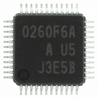
IC M16C MCU FLASH 48K 48LQFP
Manufacturer
Renesas Electronics America
Series
M16C™ M16C/Tiny/26r
Datasheet
1.M30260F3AGPU5A.pdf
(354 pages)
Specifications of M30260F6AGP#U5A
Core Processor
M16C/60
Core Size
16-Bit
Speed
20MHz
Connectivity
I²C, IEBus, SIO, UART/USART
Peripherals
DMA, PWM, Voltage Detect, WDT
Number Of I /o
39
Program Memory Size
48KB (48K x 8)
Program Memory Type
FLASH
Ram Size
2K x 8
Voltage - Supply (vcc/vdd)
2.7 V ~ 5.5 V
Data Converters
A/D 12x10b
Oscillator Type
Internal
Operating Temperature
-20°C ~ 85°C
Package / Case
48-LQFP
Cpu Family
R8C
Device Core Size
16b
Frequency (max)
20MHz
Interface Type
UART
Total Internal Ram Size
2KB
# I/os (max)
39
Number Of Timers - General Purpose
8
Operating Supply Voltage (typ)
3.3/5V
Operating Supply Voltage (max)
5.5V
Operating Supply Voltage (min)
3V
On-chip Adc
12-chx10-bit
Instruction Set Architecture
CISC
Operating Temp Range
-20C to 85C
Operating Temperature Classification
Commercial
Mounting
Surface Mount
Pin Count
48
Package Type
LQFP
Package
48LQFP
Family Name
R8C
Maximum Speed
20 MHz
Operating Supply Voltage
3.3|5 V
Data Bus Width
16 Bit
Number Of Programmable I/os
39
Number Of Timers
8
For Use With
R0K33026AS000BE - KIT DEV EVALUATION M16C/26A
Lead Free Status / RoHS Status
Lead free / RoHS Compliant
Eeprom Size
-
Lead Free Status / Rohs Status
Compliant
Available stocks
Company
Part Number
Manufacturer
Quantity
Price

Part Number:
M30260F6AGP#U5AM30260F6AGP#D3
Manufacturer:
Renesas Electronics America
Quantity:
10 000
Part Number:
M30260F6AGP#U5AM30260F6AGP#U3
Manufacturer:
Renesas Electronics America
Quantity:
10 000
Part Number:
M30260F6AGP#U5AM30260F6AGP#U3A
Manufacturer:
Renesas Electronics America
Quantity:
10 000


R
R
M
17.4 CPU Rewrite Mode
e
E
1
. v
J
6
NOTES:
0
Operation mode
Area where
rewrite control
program can be placed
Area where
rewrite control
program can be
executed
Area which can be
rewritten
Software command
Restrictions
Mode after programming Read Status Register mode
or erasing
CPU state during auto-
write and auto-erase
Flash memory status
detection
Condition for transferring
C
In CPU rewrite mode, the user ROM area can be rewritten when the CPU executes software commands.
Therefore, the user ROM area can be rewritten directly while the microcomputer is mounted on-board
without using a ROM programmer, etc. Verify the Program and the Block Erase commands are executed
only on blocks in the user ROM area.
For interrupts requested during an erasing operation in CPU rewrite mode, the M16C/26A Group flash
module offers an erase-suspend function which the erasing operation to be suspended, and access made
available to the flash. Erase-write 0 (EW0) mode and erase-write 1 (EW1) mode are provided as CPU
rewrite mode. Table 17.4.1 shows the differences between erase-write 0 (EW0) and erase-write 1 (EW1)
modes. 1 wait is required for the CPU erase-write control.
Table 17.4.1. EW0 Mode and EW1 Mode
to erase-suspend
2
9
0 .
B
2 /
1. Do not generate a DMA transfer.
2. Block 1 and 0 are enabled to rewrite by setting the FMR02 bit in the FMR0 register to "1" and
3. The time, until entering erase suspend and reading flash is enabled, is maximum td (SR-ES) after
0
0
6
2
setting the FMR16 bit in the FMR1 register to "1". Block 2 to 3 are enabled to rewrite by setting the
FMR16 bit in the FMR1 register to "1".
satisfying the conditions.
A
0
F
2
e
G
0 -
b
Item
o r
1 .
2
(2)
0
, 5
u
0
p
2
(
0
M
0
7
1
(3)
6
C
page 237
2 /
6
, A
Single chip mode
User ROM area
The rewrite control program must be The rewrite control program can be
transferred to any area other than
the flash memory (e.g., RAM) before
being executed
User ROM area
None
Operation
• Read the FMR00, FMR06 and
• Execute the read status register
Set the FMR40 and FMR41 bits in
the FMR4 register to "1" by program. is set to "1" and the interrupt request of
M
FMR07 bits in the FMR0 register by FMR06, and FMR07 bits in a program
a program
command and read the SR7, SR5
and SR4 bits
1
f o
6
C
3
2
2 /
9
6
, B
EW0 mode
M
1
6
C
2 /
6
) T
Single chip mode
User ROM area
executed in the user ROM area
User ROM area
However, this excludes blocks
with the rewrite control program
• Program, block erase command
• Read status register command
Read Array mode
Hold state (I/O ports retain the state
before the command is executed
(1)
Read the FMR0 register's FMR00,
The FMR40 bit in the FMR4 register
Cannot be executed in a block having
the rewrite control program
Can not be used
EW1 mode
17. Flash Memory Version
Related parts for M30260F6AGP#U5A
Image
Part Number
Description
Manufacturer
Datasheet
Request
R

Part Number:
Description:
KIT STARTER FOR M16C/29
Manufacturer:
Renesas Electronics America
Datasheet:

Part Number:
Description:
KIT STARTER FOR R8C/2D
Manufacturer:
Renesas Electronics America
Datasheet:

Part Number:
Description:
R0K33062P STARTER KIT
Manufacturer:
Renesas Electronics America
Datasheet:

Part Number:
Description:
KIT STARTER FOR R8C/23 E8A
Manufacturer:
Renesas Electronics America
Datasheet:

Part Number:
Description:
KIT STARTER FOR R8C/25
Manufacturer:
Renesas Electronics America
Datasheet:

Part Number:
Description:
KIT STARTER H8S2456 SHARPE DSPLY
Manufacturer:
Renesas Electronics America
Datasheet:

Part Number:
Description:
KIT STARTER FOR R8C38C
Manufacturer:
Renesas Electronics America
Datasheet:

Part Number:
Description:
KIT STARTER FOR R8C35C
Manufacturer:
Renesas Electronics America
Datasheet:

Part Number:
Description:
KIT STARTER FOR R8CL3AC+LCD APPS
Manufacturer:
Renesas Electronics America
Datasheet:
Part Number:
Description:
KIT STARTER FOR RX610
Manufacturer:
Renesas Electronics America
Datasheet:

Part Number:
Description:
KIT STARTER FOR R32C/118
Manufacturer:
Renesas Electronics America
Datasheet:

Part Number:
Description:
KIT DEV RSK-R8C/26-29
Manufacturer:
Renesas Electronics America
Datasheet:

Part Number:
Description:
KIT STARTER FOR SH7124
Manufacturer:
Renesas Electronics America
Datasheet:

Part Number:
Description:
KIT STARTER FOR H8SX/1622
Manufacturer:
Renesas Electronics America
Datasheet:

Part Number:
Description:
KIT DEV FOR SH7203
Manufacturer:
Renesas Electronics America
Datasheet: