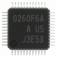
M30260F6AGP#U5A Renesas Electronics America, M30260F6AGP#U5A Datasheet - Page 120

M30260F6AGP#U5A
Manufacturer Part Number
M30260F6AGP#U5A
Description
IC M16C MCU FLASH 48K 48LQFP
Manufacturer
Renesas Electronics America
Series
M16C™ M16C/Tiny/26r
Datasheet
1.M30260F3AGPU5A.pdf
(354 pages)
Specifications of M30260F6AGP#U5A
Core Processor
M16C/60
Core Size
16-Bit
Speed
20MHz
Connectivity
I²C, IEBus, SIO, UART/USART
Peripherals
DMA, PWM, Voltage Detect, WDT
Number Of I /o
39
Program Memory Size
48KB (48K x 8)
Program Memory Type
FLASH
Ram Size
2K x 8
Voltage - Supply (vcc/vdd)
2.7 V ~ 5.5 V
Data Converters
A/D 12x10b
Oscillator Type
Internal
Operating Temperature
-20°C ~ 85°C
Package / Case
48-LQFP
Cpu Family
R8C
Device Core Size
16b
Frequency (max)
20MHz
Interface Type
UART
Total Internal Ram Size
2KB
# I/os (max)
39
Number Of Timers - General Purpose
8
Operating Supply Voltage (typ)
3.3/5V
Operating Supply Voltage (max)
5.5V
Operating Supply Voltage (min)
3V
On-chip Adc
12-chx10-bit
Instruction Set Architecture
CISC
Operating Temp Range
-20C to 85C
Operating Temperature Classification
Commercial
Mounting
Surface Mount
Pin Count
48
Package Type
LQFP
Package
48LQFP
Family Name
R8C
Maximum Speed
20 MHz
Operating Supply Voltage
3.3|5 V
Data Bus Width
16 Bit
Number Of Programmable I/os
39
Number Of Timers
8
For Use With
R0K33026AS000BE - KIT DEV EVALUATION M16C/26A
Lead Free Status / RoHS Status
Lead free / RoHS Compliant
Eeprom Size
-
Lead Free Status / Rohs Status
Compliant
Available stocks
Company
Part Number
Manufacturer
Quantity
Price
Part Number:
M30260F6AGP#U5AM30260F6AGP#D3
Manufacturer:
Renesas Electronics America
Quantity:
10 000
Part Number:
M30260F6AGP#U5AM30260F6AGP#U3
Manufacturer:
Renesas Electronics America
Quantity:
10 000
Part Number:
M30260F6AGP#U5AM30260F6AGP#U3A
Manufacturer:
Renesas Electronics America
Quantity:
10 000
- Current page: 120 of 354
- Download datasheet (4Mb)
R
R
M
e
E
1
. v
J
Figure 12.1.2.2. TA2MR to TA4MR Registers in Event Counter Mode (when using two-phase
6
0
C
2
9
0 .
B
2 /
0
0
6
2
A
0
Timer Ai mode register (i=2 to 4)
(When using two-phase pulse signal processing)
F
NOTES:
2
e
G
1. TCK1 bit is valid for timer A3 mode register. No matter how this bit is set, Timers A2 and A4 always operate in
2. If two-phase pulse signal processing is desired, following register settings are required:
0 -
b
b6
1 .
o r
• Set the TAiP bit in the UDF register to “1” (two-phase pulse signal processing function enabled).
• Set the TAiTGH and TAiTGL bits in the TRGSR register to ‘00
• Set the port direction bits for TAi
2
normal processing mode and x4 processing mode, respectively.
0
, 5
u
b5
0
0
p
2
b4
1
0
(
pulse signal processing with timer A2, A3 or A4)
M
0
7
b3
1
0
6
page 101
C
b2
0
2 /
b1
0 1
6
, A
b0
M
Bit symbol
1
f o
TMOD0
TMOD1
6
TCK0
TCK1
MR0
MR1
MR2
MR3
C
3
TA2MR to TA4MR
2
2 /
9
6
Symbol
IN
, B
and TAi
M
Operation mode select bit
To use two-phase pulse signal processing, set this bit to “0”.
Count operation type
select bit
Two-phase pulse signal
processing operation
select bit (1, 2)
To use two-phase pulse signal processing, set this bit to “0”.
To use two-phase pulse signal processing, set this bit to “1”.
To use two-phase pulse signal processing, set this bit to “0”.
1
6
C
OUT
2 /
Bit name
to “0” (input mode).
6
) T
0398
Address
16
to 039A
2
’ (TAiIN pin input).
b1 b0
0 1 : Event counter mode
0 : Reload type
1 : Free-run type
0 : Normal processing operation
1 : Multiply-by-4 processing operation
16
After reset
00
16
Function
RW
RW
RW
RW
RW
RW
RW
RW
RW
12. Timer
Related parts for M30260F6AGP#U5A
Image
Part Number
Description
Manufacturer
Datasheet
Request
R

Part Number:
Description:
KIT STARTER FOR M16C/29
Manufacturer:
Renesas Electronics America
Datasheet:

Part Number:
Description:
KIT STARTER FOR R8C/2D
Manufacturer:
Renesas Electronics America
Datasheet:

Part Number:
Description:
R0K33062P STARTER KIT
Manufacturer:
Renesas Electronics America
Datasheet:

Part Number:
Description:
KIT STARTER FOR R8C/23 E8A
Manufacturer:
Renesas Electronics America
Datasheet:

Part Number:
Description:
KIT STARTER FOR R8C/25
Manufacturer:
Renesas Electronics America
Datasheet:

Part Number:
Description:
KIT STARTER H8S2456 SHARPE DSPLY
Manufacturer:
Renesas Electronics America
Datasheet:

Part Number:
Description:
KIT STARTER FOR R8C38C
Manufacturer:
Renesas Electronics America
Datasheet:

Part Number:
Description:
KIT STARTER FOR R8C35C
Manufacturer:
Renesas Electronics America
Datasheet:

Part Number:
Description:
KIT STARTER FOR R8CL3AC+LCD APPS
Manufacturer:
Renesas Electronics America
Datasheet:

Part Number:
Description:
KIT STARTER FOR RX610
Manufacturer:
Renesas Electronics America
Datasheet:

Part Number:
Description:
KIT STARTER FOR R32C/118
Manufacturer:
Renesas Electronics America
Datasheet:

Part Number:
Description:
KIT DEV RSK-R8C/26-29
Manufacturer:
Renesas Electronics America
Datasheet:

Part Number:
Description:
KIT STARTER FOR SH7124
Manufacturer:
Renesas Electronics America
Datasheet:

Part Number:
Description:
KIT STARTER FOR H8SX/1622
Manufacturer:
Renesas Electronics America
Datasheet:

Part Number:
Description:
KIT DEV FOR SH7203
Manufacturer:
Renesas Electronics America
Datasheet:


