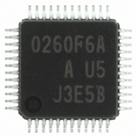
M30260F6AGP#U5A Renesas Electronics America, M30260F6AGP#U5A Datasheet - Page 159

M30260F6AGP#U5A
Manufacturer Part Number
M30260F6AGP#U5A
Description
IC M16C MCU FLASH 48K 48LQFP
Manufacturer
Renesas Electronics America
Series
M16C™ M16C/Tiny/26r
Datasheet
1.M30260F3AGPU5A.pdf
(354 pages)
Specifications of M30260F6AGP#U5A
Core Processor
M16C/60
Core Size
16-Bit
Speed
20MHz
Connectivity
I²C, IEBus, SIO, UART/USART
Peripherals
DMA, PWM, Voltage Detect, WDT
Number Of I /o
39
Program Memory Size
48KB (48K x 8)
Program Memory Type
FLASH
Ram Size
2K x 8
Voltage - Supply (vcc/vdd)
2.7 V ~ 5.5 V
Data Converters
A/D 12x10b
Oscillator Type
Internal
Operating Temperature
-20°C ~ 85°C
Package / Case
48-LQFP
Cpu Family
R8C
Device Core Size
16b
Frequency (max)
20MHz
Interface Type
UART
Total Internal Ram Size
2KB
# I/os (max)
39
Number Of Timers - General Purpose
8
Operating Supply Voltage (typ)
3.3/5V
Operating Supply Voltage (max)
5.5V
Operating Supply Voltage (min)
3V
On-chip Adc
12-chx10-bit
Instruction Set Architecture
CISC
Operating Temp Range
-20C to 85C
Operating Temperature Classification
Commercial
Mounting
Surface Mount
Pin Count
48
Package Type
LQFP
Package
48LQFP
Family Name
R8C
Maximum Speed
20 MHz
Operating Supply Voltage
3.3|5 V
Data Bus Width
16 Bit
Number Of Programmable I/os
39
Number Of Timers
8
For Use With
R0K33026AS000BE - KIT DEV EVALUATION M16C/26A
Lead Free Status / RoHS Status
Lead free / RoHS Compliant
Eeprom Size
-
Lead Free Status / Rohs Status
Compliant
Available stocks
Company
Part Number
Manufacturer
Quantity
Price
Part Number:
M30260F6AGP#U5AM30260F6AGP#D3
Manufacturer:
Renesas Electronics America
Quantity:
10 000
Part Number:
M30260F6AGP#U5AM30260F6AGP#U3
Manufacturer:
Renesas Electronics America
Quantity:
10 000
Part Number:
M30260F6AGP#U5AM30260F6AGP#U3A
Manufacturer:
Renesas Electronics America
Quantity:
10 000
- Current page: 159 of 354
- Download datasheet (4Mb)
R
R
M
e
E
. v
1
J
Figure 13.1.8. U2SMR register and U2SMR2 register
6
0
2
9
C
0 .
B
2 /
0
0
2
6
0
A
F
NOTES:
UART2 Special Mode Register
2
b7 b6 b5 b4 b3 b2 b1 b0
e
UART2 Special Mode Register 2
b7 b6 b5 b4 b3 b2 b1 b0
0 -
G
1: The BBS bit is set to “0” by writing “0" by program. (Writing “1” has no effect).
2: When a transfer begins, the SSS bit is set to “0” (Not synchronized to R
b
1 .
2
o r
0
, 5
u
0
p
2
0
(
M
0
7
0
1
6
C
page 140
2 /
6
, A
ABSCS
Symbol
ACSE
SSS
ABC
BBS
(b3)
(b7)
M
IICM
IICM2
CSC
SWC
ALS
STAC
SWC2
SDHI
Bit
Symbol
f o
1
(b7)
Bit
6
3
C
2
Symbol
U2SMR2
I
Arbitration lost detecting
flag control bit
Bus busy flag
Reserved bit
Bus collision detect
sampling clock select bit
Auto clear function
select bit of transmit
enable bit
Transmit start condition
select bit
2 /
2
Nothing is assigned. When write, set “0”.
When read, its content is indeterminate.
9
Symbol
U2SMR
C bus mode select bit
6
I C bus mode select bit 2
Clock-synchronous bit
SCL
SDA
UART initialization bit
SCL
SDA
Nothing is assigned. When write, set “0”.
When read, its content is indeterminate.
2
, B
2
2
Bit Name
2
2
M
wait output bit
wait output bit 2
output stop bit
output disable bit
1
Bit Name
6
C
2 /
Address
0376
6
) T
Address
0377
16
0 : Rising edge of transfer clock
1 : Underflow signal of timer A0
0 : Not synchronized to R
1 : Synchronized to R
0 : No auto clear function
1 : Auto clear at occurrence of bus collision
16
0 : Other than I
1 : I
0 : Update per bit
1 : Update per byte
0 : STOP condition detected
1 : START condition detected (busy)
Set to “0”
2
C bus mode
Refer to Table 13.12
0 : Disabled
1 : Enabled
0 : Disabled
1 : Enabled
0 : Disabled
1 : Enabled
0 : Disabled
1 : Enabled
0: Transfer clock
1: “L” output
0: Enabled
1: Disabled (high impedance)
X
Di).
After Reset
X0000000
2
C bus mode
After Reset
X0000000
X
2
Di
X
(2)
Di
2
Function
Function
RW
RW
RW
RW
RW
RW
RW
RW
RW
RW
RW
RW
RW
RW
RW
RW
13. Serial I/O
(1)
Related parts for M30260F6AGP#U5A
Image
Part Number
Description
Manufacturer
Datasheet
Request
R

Part Number:
Description:
KIT STARTER FOR M16C/29
Manufacturer:
Renesas Electronics America
Datasheet:

Part Number:
Description:
KIT STARTER FOR R8C/2D
Manufacturer:
Renesas Electronics America
Datasheet:

Part Number:
Description:
R0K33062P STARTER KIT
Manufacturer:
Renesas Electronics America
Datasheet:

Part Number:
Description:
KIT STARTER FOR R8C/23 E8A
Manufacturer:
Renesas Electronics America
Datasheet:

Part Number:
Description:
KIT STARTER FOR R8C/25
Manufacturer:
Renesas Electronics America
Datasheet:

Part Number:
Description:
KIT STARTER H8S2456 SHARPE DSPLY
Manufacturer:
Renesas Electronics America
Datasheet:

Part Number:
Description:
KIT STARTER FOR R8C38C
Manufacturer:
Renesas Electronics America
Datasheet:

Part Number:
Description:
KIT STARTER FOR R8C35C
Manufacturer:
Renesas Electronics America
Datasheet:

Part Number:
Description:
KIT STARTER FOR R8CL3AC+LCD APPS
Manufacturer:
Renesas Electronics America
Datasheet:

Part Number:
Description:
KIT STARTER FOR RX610
Manufacturer:
Renesas Electronics America
Datasheet:

Part Number:
Description:
KIT STARTER FOR R32C/118
Manufacturer:
Renesas Electronics America
Datasheet:

Part Number:
Description:
KIT DEV RSK-R8C/26-29
Manufacturer:
Renesas Electronics America
Datasheet:

Part Number:
Description:
KIT STARTER FOR SH7124
Manufacturer:
Renesas Electronics America
Datasheet:

Part Number:
Description:
KIT STARTER FOR H8SX/1622
Manufacturer:
Renesas Electronics America
Datasheet:

Part Number:
Description:
KIT DEV FOR SH7203
Manufacturer:
Renesas Electronics America
Datasheet:


