HW-V5-ML555-G Xilinx Inc, HW-V5-ML555-G Datasheet - Page 89
HW-V5-ML555-G
Manufacturer Part Number
HW-V5-ML555-G
Description
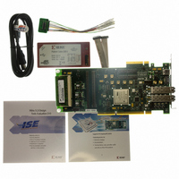
BOARD EVAL FOR VIRTEX-5 ML555
Manufacturer
Xilinx Inc
Series
Virtex™ -5r
Type
FPGAr
Datasheet
1.HW-V5-PCIE2-UNI-G.pdf
(108 pages)
Specifications of HW-V5-ML555-G
Contents
Board, Cables, CD
Silicon Manufacturer
Xilinx
Features
Parallel Connectivity, Three On-board Clock Sources
Kit Contents
Board, Cables, CD, Power Supply
Silicon Family Name
Virtex-5
Silicon Core Number
XC5VLX50T-1FF1136
Rohs Compliant
Yes
Lead Free Status / RoHS Status
Lead free / RoHS Compliant
For Use With/related Products
Virtex™-5 FPGA
For Use With
HW-AFX-SMA-SFP - CONVERSION MODULE SMA - SFPHW-AFX-SMA-SATA - CONVERSION MODULE SMA - SATAHW-AFX-SMA-RJ45 - CONVERSION MODULE SMA - RJ45HW-AFX-SMA-HSSDC2 - CONVERSION MODULE SMA - HSSDC2HW-AFX-BERG-EPHY - DAUGHTER CARD PHY BERG-EPHY
Lead Free Status / RoHS Status
Lead free / RoHS Compliant, Lead free / RoHS Compliant
Other names
122-1586
HW-V5-ML555-G
HW-V5-ML555-G
Available stocks
Company
Part Number
Manufacturer
Quantity
Price


Configuration Modes
JTAG Chain
Virtex-5 FPGA ML555 Development Kit
UG201 (v1.4) March 10, 2008
R
Table 4-1
the Configuration Mode switch (SW5).
Table 4-1: Configuration Modes
Figure 4-2
voltage level applied to the HSWAPEN input pin in the FPGA configuration bank. If the
switch is in the OFF position, the weak preconfiguration I/O pull-up resistors are disabled.
If the switch is in the ON position, the weak preconfiguration I/O pull-up resistors are
enabled.
Figure 4-3
following sources:
•
•
The JTAG chain supports bypassing of the CPLD or the Platform Flash devices. The FPGA
cannot be bypassed. Board connector/header P39 is used to enable or bypass the CPLD,
Notes:
1. Switch position 4 is used to select the DC voltage level applied to the HSWAPEN FPGA configuration
2. 0 = switch position is Closed or in the ON position. 1 = switch position is Open or in the OFF position.
3. When using SelectMAP configuration mode, see
Master SelectMAP
Slave SelectMAP
JTAG
Master Serial
Slave Serial
input. This switch controls whether the weak pull-up resistors on the FPGA I/Os are enabled or
disabled prior to configuration.
See
master mode operation. Slave SelectMAP clocking is not supported on the ML555 board. Master
SelectMAP, with a minimum 20 MHz configuration clock (CCLK) frequency, is the recommended
configuration method for PCI, PCI-X, and PCI Express applications utilizing the ML555 board.
Xilinx Parallel Cable IV or Platform Cable USB
Other JTAG cables
Figure
shows the Virtex-5 FPGA configuration modes along with the correct settings for
shows the Configuration Mode switch. SW5 position 4 is used to select the DC
shows the JTAG chain on the ML555 board. The chain can be driven by the
Mode
4-2.
(1)
(3)
(3)
Figure 4-2: Configuration Mode Switch
www.xilinx.com
Logic
0
JTAG P5
N/A
N/A
N/A
N/A
Yes
MODE
SW5
Table 4-7
UG201_c4_02_091706
(M0)
for configuration of the CCLK source for
1
0
0
1
0
1
Logic
1
Mode SW5
(M1)
Configuration Modes
2
0
1
0
0
1
(2)
(M2)
3
1
1
1
0
1
89
Related parts for HW-V5-ML555-G
Image
Part Number
Description
Manufacturer
Datasheet
Request
R

Part Number:
Description:
EVAL PLATFORM V5 FXT
Manufacturer:
Xilinx Inc
Datasheet:

Part Number:
Description:
BOARD EVAL FOR VIRTEX-5
Manufacturer:
Xilinx Inc
Datasheet:
Part Number:
Description:
BOARD EVAL FOR VIRTEX-5
Manufacturer:
Xilinx Inc
Datasheet:

Part Number:
Description:
EVALUATION PLATFORM VIRTEX-5
Manufacturer:
Xilinx Inc
Datasheet:

Part Number:
Description:
EVALUATION PLATFORM VIRTEX-5
Manufacturer:
Xilinx Inc
Datasheet:
Part Number:
Description:
KIT DEV PCIEXPRESS GTX VIRTEX5
Manufacturer:
Xilinx Inc
Datasheet:

Part Number:
Description:
EVALUATION PLATFORM VIRTEX-5
Manufacturer:
Xilinx Inc
Datasheet:
Part Number:
Description:
BOARD EVAL FOR VIRTEX-5 ML510
Manufacturer:
Xilinx Inc
Datasheet:
Part Number:
Description:
EVALUATION PLATFORM VIRTEX-5
Manufacturer:
Xilinx Inc
Datasheet:
Part Number:
Description:
CoolRunner-II CPLD
Manufacturer:
XILINX [Xilinx, Inc]
Datasheet:
Part Number:
Description:
In-System Programmable CPLD
Manufacturer:
XILINX [Xilinx, Inc]
Datasheet:
Part Number:
Description:
High-Performance CPLD
Manufacturer:
XILINX [Xilinx, Inc]
Datasheet:
Part Number:
Description:
XCR3128XL 128 Macrocell CPLD
Manufacturer:
XILINX [Xilinx, Inc]
Datasheet:
Part Number:
Description:
XC95288XL High Performance CPLD
Manufacturer:
XILINX [Xilinx, Inc]
Datasheet: