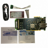
HW-V5-ML555-G Xilinx Inc, HW-V5-ML555-G Datasheet - Page 67

HW-V5-ML555-G
Manufacturer Part Number
HW-V5-ML555-G
Description
BOARD EVAL FOR VIRTEX-5 ML555
Manufacturer
Xilinx Inc
Series
Virtex™ -5r
Type
FPGAr
Datasheet
1.HW-V5-PCIE2-UNI-G.pdf
(108 pages)
Specifications of HW-V5-ML555-G
Contents
Board, Cables, CD
Silicon Manufacturer
Xilinx
Features
Parallel Connectivity, Three On-board Clock Sources
Kit Contents
Board, Cables, CD, Power Supply
Silicon Family Name
Virtex-5
Silicon Core Number
XC5VLX50T-1FF1136
Rohs Compliant
Yes
Lead Free Status / RoHS Status
Lead free / RoHS Compliant
For Use With/related Products
Virtex™-5 FPGA
For Use With
HW-AFX-SMA-SFP - CONVERSION MODULE SMA - SFPHW-AFX-SMA-SATA - CONVERSION MODULE SMA - SATAHW-AFX-SMA-RJ45 - CONVERSION MODULE SMA - RJ45HW-AFX-SMA-HSSDC2 - CONVERSION MODULE SMA - HSSDC2HW-AFX-BERG-EPHY - DAUGHTER CARD PHY BERG-EPHY
Lead Free Status / RoHS Status
Lead free / RoHS Compliant, Lead free / RoHS Compliant
Other names
122-1586
HW-V5-ML555-G
HW-V5-ML555-G
Available stocks
Company
Part Number
Manufacturer
Quantity
Price
Virtex-5 FPGA ML555 Development Kit
UG201 (v1.4) March 10, 2008
R
Table 3-24
the switch positions assigned for the M and N constants. When the switch is in the ON
position, a logic “1” is obtained, and in the OFF position, a logic “0” is obtained.
Figure 3-12
positions are used for the M and N input values to the clock synthesizers. When the switch
is in the OFF position a logic 0 is selected. When the switch is not in the OFF position, a
logic 1 is selected. ICS1 input N1 is located on SW12 position 8.
examples: one with ICS1 generating a 330 MHz clock and the other with ICS2 generating a
150 MHz clock.
Table 3-24: M and N Constant Values Set Through ML555 DIP Switch Configuration
Notes:
1. The parallel load pushbutton switch must be pressed and released to perform a parallel load of the
Parallel Load Pushbutton
synthesizer. Alternatively, the FPGA PLOAD1 or PLOAD2 output can be asserted and deasserted to
perform a parallel load without having to press and release the pushbutton switch associated with the
clock synthesizer.
Switch Position
shows the board DIP switch settings for the two clock synthesizer circuits and
shows a graphic representation of the DIP switches and indicates which switch
M8
M7
M6
M5
M4
M3
M2
M1
M0
N1
N0
www.xilinx.com
(1)
Synthesizer Circuit 1
SW10 pins 7-10
SW10 pins 6-11
SW10 pins 5-12
SW10 pins 4-13
SW10 pins 3-14
SW10 pins 2-15
SW10 pins 1-16
SW12 pins 8-9
SW10 pins 8-9
Tied to logic 0
Tied to logic 0
SW9
Figure 3-12
Synthesizer Circuit 2
SW12 pins 7-10
SW12 pins 6-11
SW12 pins 5-12
SW12 pins 4-13
SW12 pins 3-14
SW12 pins 2-15
SW12 pins 1-16
Tied to logic 0
Tied to logic 0
Tied to logic 0
Tied to logic 0
Clock Generation
SW11
shows two
67


