HW-V5-ML555-G Xilinx Inc, HW-V5-ML555-G Datasheet - Page 59
HW-V5-ML555-G
Manufacturer Part Number
HW-V5-ML555-G
Description
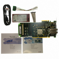
BOARD EVAL FOR VIRTEX-5 ML555
Manufacturer
Xilinx Inc
Series
Virtex™ -5r
Type
FPGAr
Datasheet
1.HW-V5-PCIE2-UNI-G.pdf
(108 pages)
Specifications of HW-V5-ML555-G
Contents
Board, Cables, CD
Silicon Manufacturer
Xilinx
Features
Parallel Connectivity, Three On-board Clock Sources
Kit Contents
Board, Cables, CD, Power Supply
Silicon Family Name
Virtex-5
Silicon Core Number
XC5VLX50T-1FF1136
Rohs Compliant
Yes
Lead Free Status / RoHS Status
Lead free / RoHS Compliant
For Use With/related Products
Virtex™-5 FPGA
For Use With
HW-AFX-SMA-SFP - CONVERSION MODULE SMA - SFPHW-AFX-SMA-SATA - CONVERSION MODULE SMA - SATAHW-AFX-SMA-RJ45 - CONVERSION MODULE SMA - RJ45HW-AFX-SMA-HSSDC2 - CONVERSION MODULE SMA - HSSDC2HW-AFX-BERG-EPHY - DAUGHTER CARD PHY BERG-EPHY
Lead Free Status / RoHS Status
Lead free / RoHS Compliant, Lead free / RoHS Compliant
Other names
122-1586
HW-V5-ML555-G
HW-V5-ML555-G
Available stocks
Company
Part Number
Manufacturer
Quantity
Price


Virtex-5 FPGA ML555 Development Kit
UG201 (v1.4) March 10, 2008
Parallel Bus Clocking (PCI Operation)
R
PCI Express applications can utilize the system board’s 100 MHz clock input on the GTP
MGTREFCLK clock input or synthesize a 100 MHz clock using the clock synthesizer, a
DCM, and GTP clocking resources. SATA applications must synthesize a 150 MHz clock
using Clock Synthesizer 2. Gigabit Ethernet applications can use either the 125 MHz
oscillator or a synthesized clock. Fibre channel applications must synthesize either a
53.125 MHz or a 106.25 MHz clock. When using the SFP connectors for Fibre channel and
Gigabit Ethernet, the REFCLK for the SFP must be either Fibre channel or Ethernet speed,
and the SMA connectors should be used to route either the Fibre channel or Ethernet
interface to an offboard connector interface.
The SMA connectors are not AC coupled on the ML555 board, so either internal GTP AC
coupling must be enabled or external AC coupling might be required for interfaces to
offboard transceivers to be electrically compatible.
The PCI specification calls for the PCI bus clock, sourced from the motherboard PCI slot, to
have one load on the add-in cards. The LogiCORE solutions for PCI and PCI-X designs,
depending upon bus mode and frequency, require that the PCI bus clock enter the FPGA
on a specific clock pin (refer to
The ML555 board PCI bus clock is implemented as follows:
•
•
•
•
If full electrical compliance is required, the designer has the option to remove one of the
two resistors (R2 or R242). As shipped, the ML555 board has both resistors installed.
The PCI bus clock (signal CLK_FROM_EDGE) enters the board on PCI edge
connector P1 pin B16.
The clock is then routed in a “Y” topology to two parallel resistors, R2 and R242.
The output side of R2 (signal PCIBUSCLK1) is routed to FPGA pin L34 (the regional
clock pin of FPGA).
The output side of R242 (signal PCIBUSCLK2) is routed to FPGA pin J14 (the global
clock pin of FPGA).
www.xilinx.com
Table
1-1).
Clock Generation
59
Related parts for HW-V5-ML555-G
Image
Part Number
Description
Manufacturer
Datasheet
Request
R

Part Number:
Description:
EVAL PLATFORM V5 FXT
Manufacturer:
Xilinx Inc
Datasheet:

Part Number:
Description:
BOARD EVAL FOR VIRTEX-5
Manufacturer:
Xilinx Inc
Datasheet:
Part Number:
Description:
BOARD EVAL FOR VIRTEX-5
Manufacturer:
Xilinx Inc
Datasheet:

Part Number:
Description:
EVALUATION PLATFORM VIRTEX-5
Manufacturer:
Xilinx Inc
Datasheet:

Part Number:
Description:
EVALUATION PLATFORM VIRTEX-5
Manufacturer:
Xilinx Inc
Datasheet:
Part Number:
Description:
KIT DEV PCIEXPRESS GTX VIRTEX5
Manufacturer:
Xilinx Inc
Datasheet:

Part Number:
Description:
EVALUATION PLATFORM VIRTEX-5
Manufacturer:
Xilinx Inc
Datasheet:
Part Number:
Description:
BOARD EVAL FOR VIRTEX-5 ML510
Manufacturer:
Xilinx Inc
Datasheet:
Part Number:
Description:
EVALUATION PLATFORM VIRTEX-5
Manufacturer:
Xilinx Inc
Datasheet:
Part Number:
Description:
CoolRunner-II CPLD
Manufacturer:
XILINX [Xilinx, Inc]
Datasheet:
Part Number:
Description:
In-System Programmable CPLD
Manufacturer:
XILINX [Xilinx, Inc]
Datasheet:
Part Number:
Description:
High-Performance CPLD
Manufacturer:
XILINX [Xilinx, Inc]
Datasheet:
Part Number:
Description:
XCR3128XL 128 Macrocell CPLD
Manufacturer:
XILINX [Xilinx, Inc]
Datasheet:
Part Number:
Description:
XC95288XL High Performance CPLD
Manufacturer:
XILINX [Xilinx, Inc]
Datasheet: