HW-V5-ML555-G Xilinx Inc, HW-V5-ML555-G Datasheet - Page 63
HW-V5-ML555-G
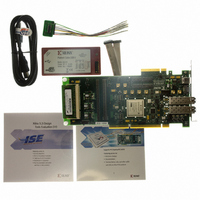
Manufacturer Part Number
HW-V5-ML555-G
Description
BOARD EVAL FOR VIRTEX-5 ML555
Manufacturer
Xilinx Inc
Series
Virtex™ -5r
Type
FPGAr
Datasheet
1.HW-V5-PCIE2-UNI-G.pdf
(108 pages)
Specifications of HW-V5-ML555-G
Contents
Board, Cables, CD
Silicon Manufacturer
Xilinx
Features
Parallel Connectivity, Three On-board Clock Sources
Kit Contents
Board, Cables, CD, Power Supply
Silicon Family Name
Virtex-5
Silicon Core Number
XC5VLX50T-1FF1136
Rohs Compliant
Yes
Lead Free Status / RoHS Status
Lead free / RoHS Compliant
For Use With/related Products
Virtex™-5 FPGA
For Use With
HW-AFX-SMA-SFP - CONVERSION MODULE SMA - SFPHW-AFX-SMA-SATA - CONVERSION MODULE SMA - SATAHW-AFX-SMA-RJ45 - CONVERSION MODULE SMA - RJ45HW-AFX-SMA-HSSDC2 - CONVERSION MODULE SMA - HSSDC2HW-AFX-BERG-EPHY - DAUGHTER CARD PHY BERG-EPHY
Lead Free Status / RoHS Status
Lead free / RoHS Compliant, Lead free / RoHS Compliant
Other names
122-1586
HW-V5-ML555-G
HW-V5-ML555-G
Available stocks
Company
Part Number
Manufacturer
Quantity
Price


Virtex-5 FPGA ML555 Development Kit
UG201 (v1.4) March 10, 2008
R
Pushbutton switch SW9 is used to parallel-load the multiplier and divisor selections for
Synthesizer 1 (U8), and switch SW11 is used to parallel-load the multiplier and divisor DIP
switch settings into Synthesizer 2 (U7). Clock synthesizer outputs are not guaranteed to be
in a known state after a power-on cycle. To establish a known clock frequency output
using the parallel mode, the switches must be configured to a valid operating range and
then the SW9 and SW11 pushbutton switches must be pressed and released. The clock
synthesizer can also be configured using FPGA outputs. The
section provides additional information.
Table 3-22
synthesizer circuit.
clock input for Clock Synthesizer 1. There are ranges below and above the VCO operating
range, which must never be selected by the user, where the VCO does not lock and an
SW10:
Parallel Load Inputs for ICS1
SW9: Parallel Load ICS1
and
Figure 3-11: Clock Synthesizer Switches (Parallel Mode)
Table 3-23
Table 3-22
show all possible values that can be generated by the clock
www.xilinx.com
shows the clock synthesis ranges with a 10 MHz reference
“Serial Mode Operation”
SW11: Parallel Load ICS2
SW12:
Parallel Load Inputs for ICS2
Clock Generation
UG201_c3_10_092706
63
Related parts for HW-V5-ML555-G
Image
Part Number
Description
Manufacturer
Datasheet
Request
R

Part Number:
Description:
EVAL PLATFORM V5 FXT
Manufacturer:
Xilinx Inc
Datasheet:

Part Number:
Description:
BOARD EVAL FOR VIRTEX-5
Manufacturer:
Xilinx Inc
Datasheet:
Part Number:
Description:
BOARD EVAL FOR VIRTEX-5
Manufacturer:
Xilinx Inc
Datasheet:

Part Number:
Description:
EVALUATION PLATFORM VIRTEX-5
Manufacturer:
Xilinx Inc
Datasheet:

Part Number:
Description:
EVALUATION PLATFORM VIRTEX-5
Manufacturer:
Xilinx Inc
Datasheet:
Part Number:
Description:
KIT DEV PCIEXPRESS GTX VIRTEX5
Manufacturer:
Xilinx Inc
Datasheet:

Part Number:
Description:
EVALUATION PLATFORM VIRTEX-5
Manufacturer:
Xilinx Inc
Datasheet:
Part Number:
Description:
BOARD EVAL FOR VIRTEX-5 ML510
Manufacturer:
Xilinx Inc
Datasheet:
Part Number:
Description:
EVALUATION PLATFORM VIRTEX-5
Manufacturer:
Xilinx Inc
Datasheet:
Part Number:
Description:
CoolRunner-II CPLD
Manufacturer:
XILINX [Xilinx, Inc]
Datasheet:
Part Number:
Description:
In-System Programmable CPLD
Manufacturer:
XILINX [Xilinx, Inc]
Datasheet:
Part Number:
Description:
High-Performance CPLD
Manufacturer:
XILINX [Xilinx, Inc]
Datasheet:
Part Number:
Description:
XCR3128XL 128 Macrocell CPLD
Manufacturer:
XILINX [Xilinx, Inc]
Datasheet:
Part Number:
Description:
XC95288XL High Performance CPLD
Manufacturer:
XILINX [Xilinx, Inc]
Datasheet: