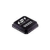
SI5325/26-EVB Silicon Laboratories Inc, SI5325/26-EVB Datasheet - Page 8

SI5325/26-EVB
Manufacturer Part Number
SI5325/26-EVB
Description
BOARD EVAL FOR SI5325/26
Manufacturer
Silicon Laboratories Inc
Specifications of SI5325/26-EVB
Main Purpose
Timing, Clock Generator
Utilized Ic / Part
SI5325, SI5326
Processor To Be Evaluated
Si5325 and Si5326
Lead Free Status / RoHS Status
Lead free / RoHS Compliant
Secondary Attributes
-
Embedded
-
Primary Attributes
-
Lead Free Status / Rohs Status
Lead free / RoHS Compliant
Si5325
1. Functional Description
The Si5325 is a low jitter, precision clock multiplier for
applications requiring clock multiplication without jitter
attenuation. The Si5325 accepts dual clock inputs
ranging from 10 to 710 MHz and generates two
synchronous clock outputs ranging from 10 to 945 MHz
and select frequencies to 1.4 GHz. The device provides
frequency translation across this operating range.
Independent dividers are available for each input clock
and output clock, so the Si5325 can accept input clocks
at different frequencies and it can generate output
clocks at different frequencies. The Si5325 input clock
frequency
programmable through an I
Laboratories
DSPLLsim, that can be used to determine the optimum
PLL divider settings for a given input frequency/clock
multiplication ratio combination that minimizes phase
noise and power consumption. This utility can be
downloaded from
Documentation).
The Si5325 is based on Silicon Laboratories' 3rd-
generation
frequency synthesis in a highly integrated PLL solution
that eliminates the need for external VCXO and loop
filter components. The Si5325 PLL loop bandwidth is
digitally programmable and supports a range from
30 kHz to 1.3 MHz. The DSPLLsim software utility can
be used to calculate valid loop bandwidth settings for a
given input clock frequency/clock multiplication ratio.
In the case when the input clocks enter alarm
conditions, the PLL will freeze the DCO output
frequency near its last value to maintain operation with
an internal state close to the last valid operating state.
The Si5325 has two differential clock outputs. The
electrical format of each clock output is independently
programmable to support LVPECL, LVDS, CML, or
CMOS loads. If not required, the second clock output
can be powered down to minimize power consumption.
In addition, the phase of one output clock may be
adjusted in relation to the phase of the other output
clock. The resolution varies from 800 ps to 2.2 ns
depending on the PLL divider settings. Consult the
DSPLLsim configuration software to determine the
phase offset resolution for a given input clock/clock
multiplication
debugging, a bypass mode is available which drives the
output clock directly from the input clock, bypassing the
internal DSPLL. The device is powered by a single 1.8,
2.5, or 3.3 V supply.
8
and
DSPLL
offers
ratio
http://www.silabs.com/timing
clock
®
combination.
a
technology,
PC-based
2
multiplication
C or SPI interface. Silicon
For
which
software
system-level
ratio
(click on
provides
Preliminary Rev. 0.4
utility,
are
1.1. Further Documentation
Consult
Precision Clock Family Reference Manual (FRM) for
detailed information about the Si5325. Additional design
support is available from Silicon Laboratories through
your distributor.
Silicon Laboratories has developed a PC-based
software utility called DSPLLsim to simplify device
configuration, including frequency planning and loop
bandwidth selection. The FRM and this utility can be
downloaded from http://www.silabs.com/timing; click on
Documentation.
the
Silicon
Laboratories
Any-Frequency


