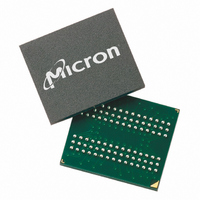
MT46H8M32LFB5-75:A TR Micron Technology Inc, MT46H8M32LFB5-75:A TR Datasheet - Page 64

MT46H8M32LFB5-75:A TR
Manufacturer Part Number
MT46H8M32LFB5-75:A TR
Description
IC DDR SDRAM 256MBIT 90VFBGA
Manufacturer
Micron Technology Inc
Datasheet
1.MT46H16M16LFBF-6A_TR.pdf
(79 pages)
Specifications of MT46H8M32LFB5-75:A TR
Format - Memory
RAM
Memory Type
Mobile DDR SDRAM
Memory Size
256M (8Mx32)
Speed
133MHz
Interface
Parallel
Voltage - Supply
1.7 V ~ 1.95 V
Operating Temperature
0°C ~ 70°C
Package / Case
90-VFBGA
Lead Free Status / RoHS Status
Contains lead / RoHS non-compliant
PDF: 09005aef82091978 / Source: 09005aef8209195b
MT46H16M16LF__2.fm - Rev. H 6/08 EN
16. MIN (
17. The I/O capacitance per DQS and DQ byte/group will not differ by more than this
18. The data valid window is derived by achieving other specifications:
19. Referenced to each output group: for x16, LDQS with DQ0–DQ7; and UDQS with
20. This limit is actually a nominal value and does not result in a fail value. CKE is HIGH
21. To maintain a valid level, the transitioning edge of the input must:
22. CK and CK# input slew rate must be ≥1 V/ns (2 V/ns if measured differentially).
23. DQ and DM input slew rates must not deviate from DQS by more than 10 percent. If
24.
25. READs and WRITEs with auto precharge are not allowed to be issued until
26. Any positive glitch must be less than 1/3 of the clock cycle and not more than +200mV
27.
28. V
29. V
30.
31. The transition times for input signals (CAS#, CKE, CS#, DM, DQ, DQS, RAS#, WE#,
32.
33. These parameters guarantee device timing, but are not tested on each device.
34. Clock must be toggled a minimum of two times during this period.
the minimum absolute value for the respective parameter.
maximum amount for any given device.
t
tion to the clock duty cycle, and a practical data valid window can be derived. The
clock is allowed a maximum duty cycle variation of 45/55. Functionality is uncertain
when operating beyond a 45/55 ratio.
DQ8–DQ15. For x32, DQS0 with DQ0–DQ7; DQS1 with DQ8–DQ15; DQS2 with DQ16–
DQ23; and DQS3 with DQ24–DQ31.
during REFRESH command period (
during standby).
the DQ/DM/DQS slew rate is less than 0.5 V/ns, timing must be derated: 50ps must
be added to
exceeds 4 V/ns, functionality is uncertain.
t
device CK and CK# inputs, collectively.
can be satisfied prior to the internal PRECHARGE command being issued.
or 2.0V, whichever is less. Any negative glitch must be less than 1/3 of the clock cycle
and not exceed either –150mV or 1.6V, whichever is more positive.
The voltage levels used are derived from a minimum
test load. In practice, the voltage levels obtained from a properly terminated bus
will provide significantly different voltage values.
cannot be greater than 1/3 of the cycle rate. V
pulse width ≤3ns, and the pulse width cannot be greater than 1/3 of the cycle rate.
t
and addresses) are measured between V
between V
t
next higher integer.
DQSQ, and
HP (MIN) is the lesser of
HZ (MAX) will prevail over
DAL = (
b. Reach at least the target AC level.
a. Sustain a constant slew rate from the current AC level through to the target AC
c. After the AC target level is reached, continue to maintain at least the target DC
IH
DD
level, V
overshoot: V
and V
level, V
t
RC or
t
WR/
DD
IH
IL
t
t
t
IL
(
(
DS and
QH (
RFC) for I
t
Q must track each other, and V
DC
AC
CK) + (
(
DC
) or V
) and V
IH
) or V
t
QH =
(MAX) = V
t
t
IH
DH for each 100 mV/ns reduction in slew rate. If slew rate
RP/
DD
IH
IL
(
t
AC
(
HP -
(
t
t
AC
DC
CK): for each term, if not already an integer, round to the
measurements is the smallest multiple of
CL minimum and
).
64
t
) for falling input signals.
DQSCK (MAX) +
).
DD
t
QHS). The data valid window derates in direct propor-
Q + 1.0V for a pulse width ≤3ns, and the pulse width
Micron Technology, Inc., reserves the right to change products or specifications without notice.
t
RFC [MIN]) else CKE is LOW (for example,
256Mb: x16, x32 Mobile DDR SDRAM
IL
(
DC
DD
t
t
) and V
CH minimum actually applied to the
IL
RPST (MAX) condition.
Q must be less than or equal to V
undershoot: V
IH
(
AC
V
DD
) for rising input signals and
©2005 Micron Technology, Inc. All rights reserved.
level and the referenced
IL
(MIN) = –1.0V for a
t
t
HP (
CK that meets
t
CK/2),
t
RAS (MIN)
Notes
DD
.


