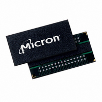
MT46H8M16LFCF-10 IT TR Micron Technology Inc, MT46H8M16LFCF-10 IT TR Datasheet - Page 25

MT46H8M16LFCF-10 IT TR
Manufacturer Part Number
MT46H8M16LFCF-10 IT TR
Description
IC DDR SDRAM 128MBIT 60VFBGA
Manufacturer
Micron Technology Inc
Datasheet
1.MT46H8M16LFCF-10.pdf
(66 pages)
Specifications of MT46H8M16LFCF-10 IT TR
Format - Memory
RAM
Memory Type
Mobile DDR SDRAM
Memory Size
128M (8Mx16)
Speed
100MHz
Interface
Parallel
Voltage - Supply
1.7 V ~ 1.9 V
Operating Temperature
-40°C ~ 85°C
Package / Case
60-VFBGA
Lead Free Status / RoHS Status
Lead free / RoHS Compliant
Figure 13:
Truncated READs
PDF: 09005aef8199c1ec/Source: 09005aef81a19319
MT46H8M16LF_1.fm - Rev. K 7/07 EN
Random READ Accesses
Notes:
Note:
COMMAND
COMMAND
COMMAND
1. D
2. BL = 4 in the cases shown (applies for bursts of 8 as well; if BL = 2, the BST command shown
3. READs are to an active row in any bank.
4. Shown with nominal
Data from any READ burst may be truncated with a BURST TERMINATE command, as
shown in Figure 14 on page 26. The burst terminate latency is equal to the READ (CAS)
latency, i.e., the BURST TERMINATE command should be issued x cycles after the READ
command, where x equals the number of desired data element pairs (pairs are required
by the 2n-prefetch architecture).
Data from any READ burst must be completed or truncated before a subsequent WRITE
command can be issued. If truncation is necessary, the BURST TERMINATE command
must be used, as shown in Figure 15 on page 27. The
t
defined in the section on WRITEs.)
A READ burst may be followed by, or truncated with, a PRECHARGE command to the
same bank provided that auto precharge was not activated. The PRECHARGE command
should be issued x cycles after the READ command, where x equals the number of
desired data element pairs (pairs are required by the n-prefetch architecture). This is
shown in Figure 16 on page 28. Following the PRECHARGE command, a subsequent
command to the same bank cannot be issued until
DQSS (MAX) case has a longer bus idle time. (
ADDRESS
ADDRESS
ADDRESS
Part of the row precharge time is hidden during the access of the last data elements.
can be a NOP).
OUT
DQS
DQS
CK#
CK#
DQ
DQ
CK
CK
n (or x, b, g) = data-out from column n (or column x, column b, column g).
READ
Bank,
READ
Bank,
Col n
Col n
T0
T0
CL = 2
t
AC,
READ
Bank,
READ
Bank,
Col x
Col x
T1
T1
t
DQSCK, and
CL = 3
25
T1n
T1n
128Mb: 8 Meg x 16 Mobile DDR SDRAM
D
OUT
n
READ
Bank,
READ
Bank,
Col b
Col b
T2
T2
Micron Technology, Inc., reserves the right to change products or specifications without notice.
t
DQSQ.
D
n + 1
OUT
T2n
T2n
t
DQSS [MIN] and
D
D
OUT
n
OUT
x
READ
Bank,
READ
Bank,
Col g
Col g
T3
T3
t
DON’T CARE
RP is met.
t
DQSS (MIN) case is shown; the
D
n + 1
D
x + 1
OUT
T3n
T3n
OUT
D
D
OUT
x
OUT
b
T4
T4
NOP
NOP
©2004 Micron Technology, Inc. All rights reserved.
t
DQSS [MAX] are
D
x + 1
D
b + 1
TRANSITIONING DATA
OUT
T4n
OUT
T4n
D
D
OUT
b
OUT
g
T5
T5
Operations
NOP
NOP
b + 1
D
D
g + 1
OUT
OUT
T5n
T5n


