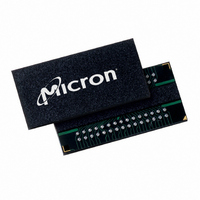
MT46H8M16LFCF-10 IT TR Micron Technology Inc, MT46H8M16LFCF-10 IT TR Datasheet - Page 10

MT46H8M16LFCF-10 IT TR
Manufacturer Part Number
MT46H8M16LFCF-10 IT TR
Description
IC DDR SDRAM 128MBIT 60VFBGA
Manufacturer
Micron Technology Inc
Datasheet
1.MT46H8M16LFCF-10.pdf
(66 pages)
Specifications of MT46H8M16LFCF-10 IT TR
Format - Memory
RAM
Memory Type
Mobile DDR SDRAM
Memory Size
128M (8Mx16)
Speed
100MHz
Interface
Parallel
Voltage - Supply
1.7 V ~ 1.9 V
Operating Temperature
-40°C ~ 85°C
Package / Case
60-VFBGA
Lead Free Status / RoHS Status
Lead free / RoHS Compliant
Burst Type
READ Latency
Figure 3:
PDF: 09005aef8199c1ec/Source: 09005aef81a19319
MT46H8M16LF_1.fm - Rev. K 7/07 EN
Standard Mode Register Definition
the most significant column address bit for a given configuration). The remaining (least
significant) address bit(s) is (are) used to select the starting location within the block.
The programmed burst length applies to both READ and WRITE bursts.
Accesses within a given burst may be programmed to be either sequential or interleaved;
this is referred to as the burst type and is selected via bit M3.
The ordering of accesses within a burst is determined by the burst length, the burst type
and the starting column address. See Table 5 on page 11 for more information.
The READ latency is the delay, in clock cycles, between the registration of a READ
command and the availability of the first bit of output data. The latency can be set to 2 or
3 clocks, as shown in Figure 3 on page 10.
For CL = 3, if the READ command is registered at clock edge n, then the data will nomi-
nally be available at (n + 2 clocks +
clock edge n, then the data will be nominally be available at (n + 1 clock +
Reserved states should not be used as unknown operation or incompatibility with future
versions may result.
M11
0
–
Should be
programmed
to “0” to ensure
compatibility with
future devices.
M13 M12
0
0
1
1
M10
0
–
0
1
0
1
M9
0
–
Mode Register Definintion
Base Mode Register
Reserved
Extended Mode Register
Resereved
M8
0
–
M13
BA1
13
0
M7
0
–
12
0
M12
BA0
Valid
11
–
A11
M11
M6
Operating Mode
0
0
0
0
1
1
1
1
10
A10
M10
M5
Normal Operation
All other states reserved
0
0
1
1
0
0
1
1
Operating Mode
10
M4
M9
A9
9
0
1
0
1
0
1
0
1
t
M8
A8
8
AC). For CL = 2, if the READ command is registered at
128Mb: 8 Meg x 16 Mobile DDR SDRAM
CAS Latency
M7
A7
7
Reserved
Reserved
Reserved
Reserved
Reserved
Reserved
Micron Technology, Inc., reserves the right to change products or specifications without notice.
CAS Latency BT
M6
2
3
A6
6
M5
5
A5
M4
4
A4
M3
A3
3
M2
Burst Length
0
0
0
0
1
1
1
1
M2
A2
2
M3
0
1
M1
0
0
1
1
0
0
1
1
M1
1
A1
M0
0
1
0
1
0
1
0
1
©2004 Micron Technology, Inc. All rights reserved.
Register Definition
A0
M0
0
Reserved
Reserved
Reserved
Reserved
Reserved
M3 = 0
Interleaved
Burst Type
Sequential
Burst Length
2
4
8
Address Bus
Mode
Register
Reserved
Reserved
Reserved
Reserved
Reserved
M3 = 1
t
AC).
2
4
8


