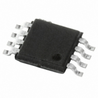
M34E02-FDW1TP STMicroelectronics, M34E02-FDW1TP Datasheet - Page 8

M34E02-FDW1TP
Manufacturer Part Number
M34E02-FDW1TP
Description
IC EEPROM 2KBIT 400KHZ 8TSSOP
Manufacturer
STMicroelectronics
Datasheet
1.M34E02-FMB1TG.pdf
(34 pages)
Specifications of M34E02-FDW1TP
Format - Memory
EEPROMs - Serial
Memory Type
EEPROM
Memory Size
2K (256 x 8)
Speed
400kHz
Interface
I²C, 2-Wire Serial
Voltage - Supply
1.7 V ~ 3.6 V
Operating Temperature
0°C ~ 70°C
Package / Case
8-TSSOP
Organization
256 K x 8
Interface Type
2-Wire
Maximum Clock Frequency
0.4 MHz
Access Time
900 ns
Supply Voltage (max)
3.6 V
Supply Voltage (min)
1.7 V
Maximum Operating Current
2 mA
Maximum Operating Temperature
+ 70 C
Mounting Style
SMD/SMT
Minimum Operating Temperature
0 C
Operating Supply Voltage
1.7 V, 3.6 V
Lead Free Status / RoHS Status
Lead free / RoHS Compliant
Other names
497-8654-2
M34E02-FDW1TP
M34E02-FDW1TP
Available stocks
Company
Part Number
Manufacturer
Quantity
Price
Company:
Part Number:
M34E02-FDW1TP
Manufacturer:
NS
Quantity:
500
Part Number:
M34E02-FDW1TP
Manufacturer:
ST
Quantity:
20 000
Signal description
2
2.1
2.2
2.3
2.4
8/34
Signal description
Serial Clock (SCL)
This input signal is used to strobe all data in and out of the device. In applications where this
signal is used by slave devices to synchronize the bus to a slower clock, the bus master
must have an open drain output, and a pull-up resistor can be connected from Serial Clock
(SCL) to V
most applications, though, this method of synchronization is not employed, and so the pull-
up resistor is not necessary, provided that the bus master has a push-pull (rather than open
drain) output.
Serial Data (SDA)
This bidirectional signal is used to transfer data in or out of the device. It is an open drain
output that may be wire-OR’ed with other open drain or open collector signals on the bus. A
pull up resistor must be connected from Serial Data (SDA) to V
the value of the pull-up resistor can be calculated).
Chip Enable (E0, E1, E2)
These input signals are used to set the value that is to be looked for on the three least
significant bits (b3, b2, b1) of the 7-bit device select code. In the end application, E0, E1 and
E2 must be directly (not through a pull-up or pull-down resistor) connected to V
establish the device select code. When these inputs are not connected, an internal pull-
down circuitry makes (E0,E1,E2) = (0,0,0).
The E0 input is used to detect the V
Figure 3.
Write Control (WC)
This input signal is provided for protecting the contents of the whole memory from
inadvertent write operations. Write Control (WC) is used to enable (when driven low) or
disable (when driven high) write instructions to the entire memory area or to the Protection
Register.
When Write Control (WC) is tied low or left unconnected, the write protection of the first half
of the memory is determined by the status of the Protection Register.
CC
Device select code
.
(Figure 4
indicates how the value of the pull-up resistor can be calculated). In
Doc ID 10367 Rev 9
E i
HV
M34E02
V CC
V SS
voltage, when decoding an SWP or CWP instruction.
E i
M34E02
V CC
V SS
Ai12301
CC
.
(Figure 4
indicates how
CC
or V
M34E02
SS
to


