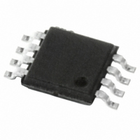
M34E02-FDW1TP STMicroelectronics, M34E02-FDW1TP Datasheet - Page 12

M34E02-FDW1TP
Manufacturer Part Number
M34E02-FDW1TP
Description
IC EEPROM 2KBIT 400KHZ 8TSSOP
Manufacturer
STMicroelectronics
Datasheet
1.M34E02-FMB1TG.pdf
(34 pages)
Specifications of M34E02-FDW1TP
Format - Memory
EEPROMs - Serial
Memory Type
EEPROM
Memory Size
2K (256 x 8)
Speed
400kHz
Interface
I²C, 2-Wire Serial
Voltage - Supply
1.7 V ~ 3.6 V
Operating Temperature
0°C ~ 70°C
Package / Case
8-TSSOP
Organization
256 K x 8
Interface Type
2-Wire
Maximum Clock Frequency
0.4 MHz
Access Time
900 ns
Supply Voltage (max)
3.6 V
Supply Voltage (min)
1.7 V
Maximum Operating Current
2 mA
Maximum Operating Temperature
+ 70 C
Mounting Style
SMD/SMT
Minimum Operating Temperature
0 C
Operating Supply Voltage
1.7 V, 3.6 V
Lead Free Status / RoHS Status
Lead free / RoHS Compliant
Other names
497-8654-2
M34E02-FDW1TP
M34E02-FDW1TP
Available stocks
Company
Part Number
Manufacturer
Quantity
Price
Company:
Part Number:
M34E02-FDW1TP
Manufacturer:
NS
Quantity:
500
Part Number:
M34E02-FDW1TP
Manufacturer:
ST
Quantity:
20 000
Device operation
3.5
12/34
Memory addressing
To start communication between the bus master and the slave device, the bus master must
initiate a Start condition. Following this, the bus master sends the device select code, shown
in
The device select code consists of a 4-bit device type identifier, and a 3-bit Chip Enable
“Address” (E2, E1, E0). To address the memory array, the 4-bit device type identifier is
1010b; to access the write-protection settings, it is 0110b.
Up to eight memory devices can be connected on a single I
unique 3-bit code on the Chip Enable (E0, E1, E2) inputs. When the device select code is
received, the device only responds if the Chip Enable address is the same as the value on
the Chip Enable (E0, E1, E2) inputs.
The 8
If a match occurs on the device select code, the corresponding device gives an
acknowledgment on Serial Data (SDA) during the 9
the device select code, it deselects itself from the bus, and goes into Standby mode.
Table 3.
1. X =
Figure 6.
Current Address Read
Random Address Read
Sequential Read
Byte Write
Page Write
Table 2
th
V
IH
bit is the Read/Write bit (RW). This bit is set to 1 for Read and 0 for Write operations.
Mode
or V
(on Serial Data (SDA), most significant bit first).
Memory
IL
Operating modes
Result of setting the write protection
.
Area
Default EEPROM memory area
state before write access
to the Protect Register
RW bit
Standard
Standard
Array
Array
1
0
1
1
0
0
Doc ID 10367 Rev 9
WC
FFh
80h
7Fh
00h
V
V
X
X
X
X
IL
IL
(1)
Bytes
16
1
1
1
1
th
Start, Device Select, RW = 1
Start, Device Select, RW = 0, Address
reStart, Device Select, RW = 1
Similar to Current or Random Address
Read
Start, Device Select, RW = 0
Start, Device Select, RW = 0
bit time. If the device does not match
State of the EEPROM memory
area after write access
to the Protect Register
2
Protected
Standard
C bus. Each one is given a
Array
Write
Array
Initial Sequence
FFh
80h
7Fh
00h
AI01936C
M34E02


