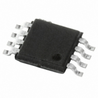
M34E02-FDW1TP STMicroelectronics, M34E02-FDW1TP Datasheet - Page 6

M34E02-FDW1TP
Manufacturer Part Number
M34E02-FDW1TP
Description
IC EEPROM 2KBIT 400KHZ 8TSSOP
Manufacturer
STMicroelectronics
Datasheet
1.M34E02-FMB1TG.pdf
(34 pages)
Specifications of M34E02-FDW1TP
Format - Memory
EEPROMs - Serial
Memory Type
EEPROM
Memory Size
2K (256 x 8)
Speed
400kHz
Interface
I²C, 2-Wire Serial
Voltage - Supply
1.7 V ~ 3.6 V
Operating Temperature
0°C ~ 70°C
Package / Case
8-TSSOP
Organization
256 K x 8
Interface Type
2-Wire
Maximum Clock Frequency
0.4 MHz
Access Time
900 ns
Supply Voltage (max)
3.6 V
Supply Voltage (min)
1.7 V
Maximum Operating Current
2 mA
Maximum Operating Temperature
+ 70 C
Mounting Style
SMD/SMT
Minimum Operating Temperature
0 C
Operating Supply Voltage
1.7 V, 3.6 V
Lead Free Status / RoHS Status
Lead free / RoHS Compliant
Other names
497-8654-2
M34E02-FDW1TP
M34E02-FDW1TP
Available stocks
Company
Part Number
Manufacturer
Quantity
Price
Company:
Part Number:
M34E02-FDW1TP
Manufacturer:
NS
Quantity:
500
Part Number:
M34E02-FDW1TP
Manufacturer:
ST
Quantity:
20 000
Description
1
6/34
Description
The M34E02 is a 2 Kbit serial EEPROM memory able to lock permanently the data in its first
half (from location 00h to 7Fh). This facility has been designed specifically for use in DRAM
DIMMs (dual interline memory modules) with serial presence detect (SPD). All the
information concerning the DDR1 or DDR2 configuration of the DRAM module (such as its
access speed, size and organization) can be kept write-protected in the first half of the
memory.
The first half of the memory area can be write-protected using two different software write
protection mechanisms. By sending the device a specific sequence, the first 128 bytes of
the memory become write protected: permanently or resettable. In addition, the device
allows the entire memory area to be write protected, using the WC input (for example by
tieing this input to V
These I
organized as 256 × 8 bits.
I
The device carries a built-in 4-bit device type identifier code (1010) in accordance with the
I
(0110) to define the protection. These codes are used together with the voltage level applied
on the three chip enable inputs (E2, E1, E0).
The device behaves as a slave device in the I
synchronized by the serial clock. Read and Write operations are initiated by a Start
condition, generated by the bus master. The Start condition is followed by a device select
code and RW bit (as described in
When writing data to the memory, the memory inserts an acknowledge bit during the 9
time, following the bus master’s 8-bit transmission. When data is read by the bus master, the
bus master acknowledges the receipt of the data byte in the same way. Data transfers are
terminated by a Stop condition after an Ack for WRITE, and after a NoAck for READ.
Figure 1.
2
2
C uses a two wire serial interface, comprising a bi-directional data line and a clock line.
C bus definition to access the memory area and a second device type identifier code
2
C-compatible electrically erasable programmable memory (EEPROM) devices are
Logic diagram
CC
).
E0-E2
SCL
WC
Doc ID 10367 Rev 9
Table
3
V CC
2), terminated by an acknowledge bit.
V SS
M34E02
2
C protocol, with all memory operations
AI09020
SDA
M34E02
th
bit


