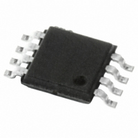
M34E02-FDW1TP STMicroelectronics, M34E02-FDW1TP Datasheet - Page 18

M34E02-FDW1TP
Manufacturer Part Number
M34E02-FDW1TP
Description
IC EEPROM 2KBIT 400KHZ 8TSSOP
Manufacturer
STMicroelectronics
Datasheet
1.M34E02-FMB1TG.pdf
(34 pages)
Specifications of M34E02-FDW1TP
Format - Memory
EEPROMs - Serial
Memory Type
EEPROM
Memory Size
2K (256 x 8)
Speed
400kHz
Interface
I²C, 2-Wire Serial
Voltage - Supply
1.7 V ~ 3.6 V
Operating Temperature
0°C ~ 70°C
Package / Case
8-TSSOP
Organization
256 K x 8
Interface Type
2-Wire
Maximum Clock Frequency
0.4 MHz
Access Time
900 ns
Supply Voltage (max)
3.6 V
Supply Voltage (min)
1.7 V
Maximum Operating Current
2 mA
Maximum Operating Temperature
+ 70 C
Mounting Style
SMD/SMT
Minimum Operating Temperature
0 C
Operating Supply Voltage
1.7 V, 3.6 V
Lead Free Status / RoHS Status
Lead free / RoHS Compliant
Other names
497-8654-2
M34E02-FDW1TP
M34E02-FDW1TP
Available stocks
Company
Part Number
Manufacturer
Quantity
Price
Company:
Part Number:
M34E02-FDW1TP
Manufacturer:
NS
Quantity:
500
Part Number:
M34E02-FDW1TP
Manufacturer:
ST
Quantity:
20 000
Initial delivery state
4
5
5.1
5.1.1
18/34
Initial delivery state
The device is delivered with all bits in the memory array set to ‘1’ (each Byte contains FFh).
Use within a DDR1/DDR2 DRAM module
In the application, the M34E02 is soldered directly in the printed circuit module. The three
Chip Enable inputs (E0, E1, E2) must be connected to V
using a pull-up or pull-down resistor) through the DIMM socket (see
resistors needed for normal behavior of the I
mother-board (as shown in
The Write Control (WC) of the M34E02 can be left unconnected. However, connecting it to
V
Table 4.
Programming the M34E02
The situations in which the M34E02 is programmed can be considered under two headings:
●
●
Isolated DRAM module
With specific programming equipment, it is possible to define the M34E02 content, using
Byte and Page Write instructions, and its write-protection using the SWP and CWP
instructions. To issue the SWP and CWP instructions, the DRAM module must be inserted
in a specific slot where the E0 signal can be driven to V
programming step is mainly intended for use by DRAM module makers, whose end
application manufacturers will want to clear this write-protection with the CWP on their own
specific programming equipment, to modify the lower 128 Bytes, and finally to set
permanently the write-protection with the PSWP instruction.
SS
is recommended, to maintain full read and write access.
when the DDR2 DRAM is isolated (not inserted on the PCB motherboard)
when the DDR2 DRAM is inserted on the PCB motherboard
DIMM position
DRAM DIMM connections
0
1
2
3
4
5
6
7
Figure
Doc ID 10367 Rev 9
11).
V
V
V
V
V
V
V
V
E2
CC
CC
CC
CC
SS
SS
SS
SS
2
C bus are connected on the I
HV
SS
during the whole instruction. This
V
V
V
V
V
V
V
V
or V
E1
CC
CC
CC
CC
SS
SS
SS
SS
CC
directly (that is without
Table
4). The pull-up
2
C bus of the
V
V
V
V
V
V
V
V
E0
CC
CC
CC
CC
SS
SS
SS
SS
M34E02


