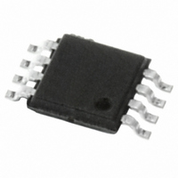
M34E02-FDW1TP STMicroelectronics, M34E02-FDW1TP Datasheet - Page 16

M34E02-FDW1TP
Manufacturer Part Number
M34E02-FDW1TP
Description
IC EEPROM 2KBIT 400KHZ 8TSSOP
Manufacturer
STMicroelectronics
Datasheet
1.M34E02-FMB1TG.pdf
(34 pages)
Specifications of M34E02-FDW1TP
Format - Memory
EEPROMs - Serial
Memory Type
EEPROM
Memory Size
2K (256 x 8)
Speed
400kHz
Interface
I²C, 2-Wire Serial
Voltage - Supply
1.7 V ~ 3.6 V
Operating Temperature
0°C ~ 70°C
Package / Case
8-TSSOP
Organization
256 K x 8
Interface Type
2-Wire
Maximum Clock Frequency
0.4 MHz
Access Time
900 ns
Supply Voltage (max)
3.6 V
Supply Voltage (min)
1.7 V
Maximum Operating Current
2 mA
Maximum Operating Temperature
+ 70 C
Mounting Style
SMD/SMT
Minimum Operating Temperature
0 C
Operating Supply Voltage
1.7 V, 3.6 V
Lead Free Status / RoHS Status
Lead free / RoHS Compliant
Other names
497-8654-2
M34E02-FDW1TP
M34E02-FDW1TP
Available stocks
Company
Part Number
Manufacturer
Quantity
Price
Company:
Part Number:
M34E02-FDW1TP
Manufacturer:
NS
Quantity:
500
Part Number:
M34E02-FDW1TP
Manufacturer:
ST
Quantity:
20 000
Device operation
3.7.3
3.8
3.8.1
3.8.2
3.8.3
16/34
Minimizing system delays by polling on ACK
During the internal Write cycle, the device disconnects itself from the bus, and writes a copy
of the data from its internal latches to the memory cells. The maximum Write time (t
shown in
can be used by the bus master.
The sequence, as shown in
●
●
●
Read operations
Read operations are performed independently of whether hardware or software protection
has been set.
The device has an internal address counter which is incremented each time a byte is read.
Random Address Read
A dummy Write is first performed to load the address into this address counter (as shown in
Figure
condition, and repeats the device select code, with the RW bit set to 1. The device
acknowledges this, and outputs the contents of the addressed byte. The bus master must
not acknowledge the byte, and terminates the transfer with a Stop condition.
Current Address Read
For the Current Address Read operation, following a Start condition, the bus master only
sends a device select code with the RW bit set to 1. The device acknowledges this, and
outputs the byte addressed by the internal address counter. The counter is then
incremented. The bus master terminates the transfer with a Stop condition, as shown in
Figure
Sequential Read
This operation can be used after a Current Address Read or a Random Address Read. The
bus master does acknowledge the data byte output, and sends additional clock pulses so
that the device continues to output the next byte in sequence. To terminate the stream of
bytes, the bus master must not acknowledge the last byte, and must generate a Stop
condition, as shown in
The output data comes from consecutive addresses, with the internal address counter
automatically incremented after each byte output. After the last memory address, the
address counter ‘rolls-over’, and the device continues to output data from memory address
00h.
Initial condition: a Write cycle is in progress.
Step 1: the bus master issues a Start condition followed by a device select code (the
first byte of the new instruction).
Step 2: if the device is busy with the internal Write cycle, no Ack will be returned and
the bus master goes back to Step 1. If the device has terminated the internal Write
cycle, it responds with an Ack, indicating that the device is ready to receive the second
part of the instruction (the first byte of this instruction having been sent during Step 1).
10) but without sending a Stop condition. Then, the bus master sends another Start
10, without acknowledging the byte.
Table
14, but the typical time is shorter. To make use of this, a polling sequence
Figure
Figure
10.
Doc ID 10367 Rev 9
9, is:
M34E02
w
) is


